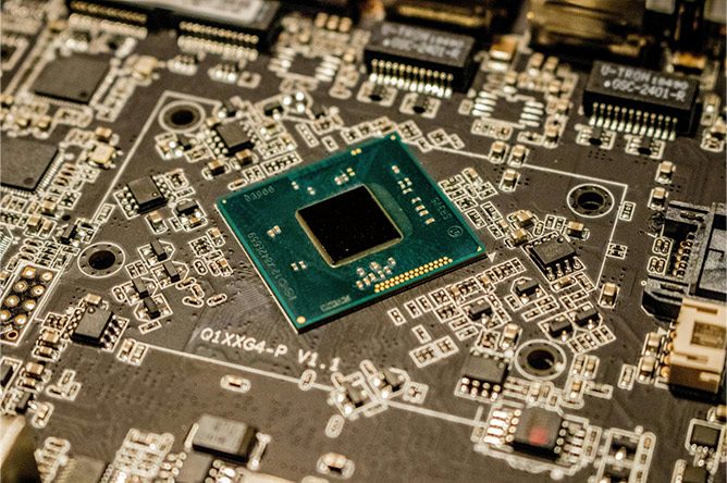
In the current era of 5G/6G high-frequency communications, AI servers, smart vehicles, and RF aerospace engineering, signal transmission rates have soared to gigabit (Gbps) and even terahertz levels. Against this backdrop, PCB transmission lines are no longer simple conductors; instead, they function as distributed parameter circuits. Any discontinuity in impedance will directly trigger signal reflection, overshoot, undershoot, and severe electromagnetic interference (EMI), ultimately leading to system-level crashes or data packet loss. This article provides an in-depth exploration of the core mechanisms behind PCB impedance control. By combining the four critical dimensions of materials, design, manufacturing processes, and quality testing, we will review the comprehensive systems engineering required for robust impedance control.
1. Engineering Extension of Basic Impedance Theory
1.1 Evolution of Definitions and Electromagnetic Wave Transmission Mechanisms
From the perspective of electromagnetic field theory (Maxwell’s equations), PCB impedance (characteristic impedance Z0) is not traditional DC resistance. Rather, it represents the ratio of the voltage wave to the current wave as high-frequency electromagnetic waves propagate through the transmission line.
- Single-Ended Impedance: This refers to the single transmission path formed by a signal line and its reference plane (ground or power layer). It carries conventional single-ended signals and is extremely sensitive to the integrity of the reference plane.
- Differential Impedance: This is designed for a pair of interleaved differential signal lines. The two lines transmit signals that are equal in magnitude but opposite in direction. Its approximate calculation formula is:
Where k represents the mutual coupling coefficient between the two lines. When the two lines are far apart and the coupling is extremely weak (k → 0), the differential impedance is exactly twice the single-ended impedance. However, in actual high-density routing, the two lines are usually tightly coupled to suppress common-mode noise and improve anti-interference capability. This makes the overall value slightly lower than twice the single-ended impedance under the same process conditions.
1.2 Deep Dissection of the Core Calculation Formula (IPC-2221 Standard)
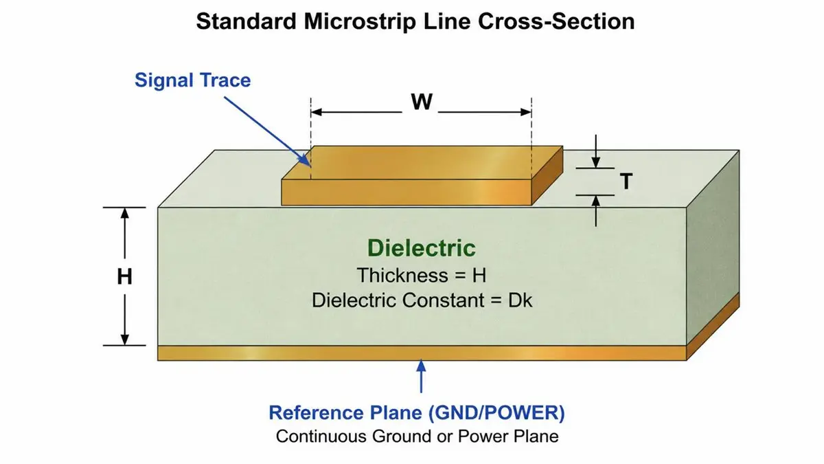
Standard Surface Microstrip Line Structure
Taking the most common surface Microstrip Line as an example, its classic analytical formula according to the IPC-2221 industry standard is as follows:
- Signal Trace Parameters: Trace Width W, Copper Thickness T
- Dielectric Parameters: Thickness H, Dielectric Constant Dk (or Er)
- Reference Layer: Reference Plane (GND/POWER)
Analysis of how variables affect impedance:
- Dielectric Thickness H (Positively Correlated, Extremely Sensitive): As H increases, the signal line moves farther away from the reference plane, reducing the distributed capacitance between the line and ground. A decrease in capacitance causes the impedance to increase sharply.
- Trace Width W and Copper Thickness T (Negatively Correlated): As W or T increases, the cross-sectional area of the transmission line expands. This not only increases the distributed capacitance to ground but also decreases the distributed inductance per unit length, causing the impedance to decrease.
- Dielectric Constant Dk (Negatively Correlated): A stronger electric polarization capability of the medium (higher Dk) results in a larger distributed capacitance, which causes the impedance to decrease.
2. Deep Analysis of Key Parameters Affecting Impedance
In actual mass production of PCBs, impedance is not a fixed value but a statistical variable in dynamic fluctuation. We must precisely control the following core parameters:
| Parameter Name | Sensitivity | Physical Variation Mechanism | Engineering Tolerance Requirement |
|---|---|---|---|
| Dielectric Thickness (H) | ★★★★★ | Resin flow inconsistency during lamination or uneven fiberglass cloth stacking causes physical thickness drift. | Core layer allows ±10%. Prepreg (PP) thickness must be strictly managed. |
| Trace Width / Spacing (W/S) | ★★★★ | Side etching effect. Flushing of chemical solution causes the actual trace to become trapezoidal (narrower at the top, wider at the bottom). | High-precision boards require a tolerance within ±0.02 mm. |
| Dielectric Constant (Dk) | ★★★★ | Fluctuations in the ratio of resin (lower Dk) to fiberglass cloth (higher Dk); variation based on signal operating frequency. | Select low-loss materials to limit Dk fluctuations within a narrow band. |
| Copper Roughness & Thickness (T) | ★★★ | High-frequency signals exhibit the skin effect, where current flows only on the copper surface. Surface roughness effectively lengthens the transmission path. | High-frequency circuits strictly require RTF (Reverse Treated Foil) or VLP (Very Low Profile) copper foil. |
| Environmental Factors | ★★★ | Excessive moisture absorption in base materials causes the overall Dk to spike, as the Dk of water is close to 80. | Implement baking mechanisms during manufacturing; use sealed, waterproof, and moisture-proof designs for end applications. |
3. PCB Material Selection and Environmental Control Chain
3.1 Material System Classification and Physical Performance Comparison
When selecting substrates, engineers must find the optimal balance between electrical performance (Dk/Df), thermal stability (Tg), and commercial cost.
| Material Type | Dk Value | Application Scenario | Core Advantages |
|---|---|---|---|
| Standard FR-4 | 4.2 – 4.8 | Consumer Electronics | Low cost, good processability |
| High-Tg FR-4 | 4.0 – 4.5 | Automotive / Industrial Control | High temperature resistance, low thermal expansion |
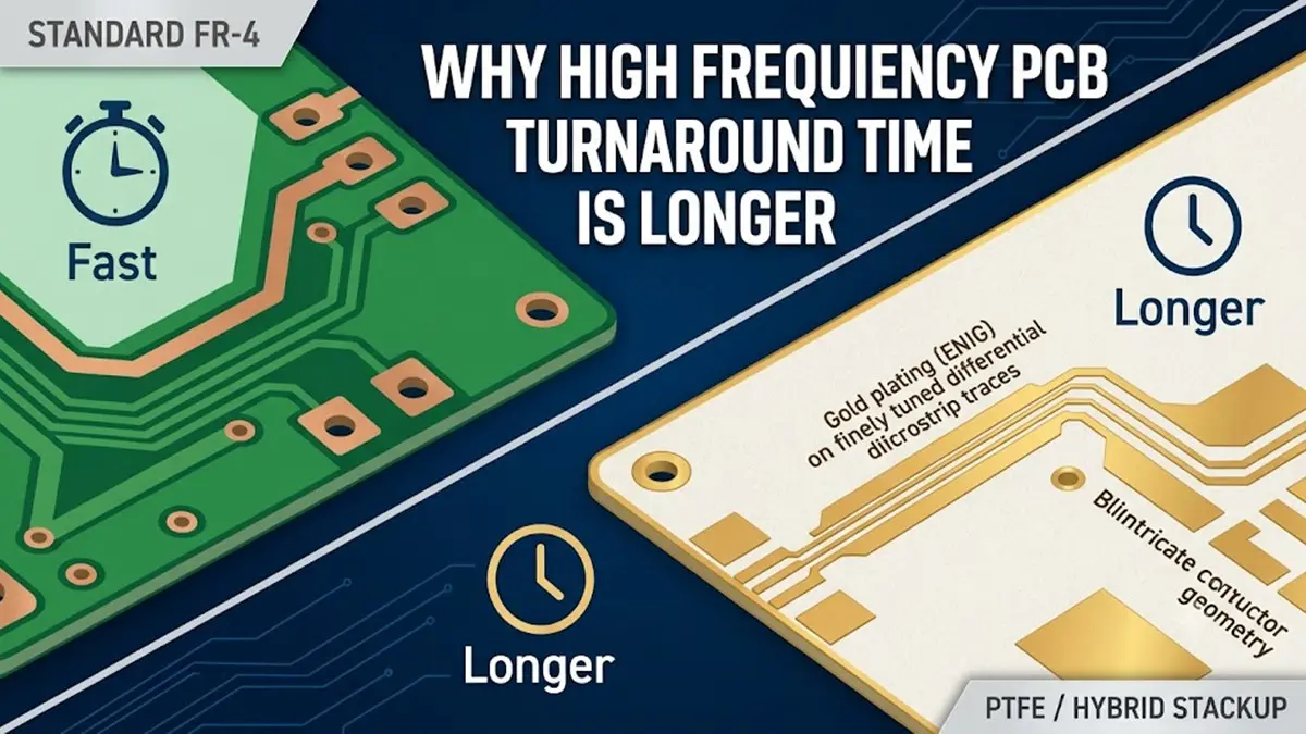
| PTFE (Polytetrafluoroethylene) | 2.0 – 2.5 | 5G / RF / Aerospace | Low loss, stable Dk |
- Standard FR-4: Composed of epoxy resin and electrical-grade fiberglass cloth. Its Dk ranges from 4.2 to 4.8, and its dissipation factor (Df) is relatively large. It is suitable for consumer electronics with lower clock frequencies that are sensitive to cost.
- High-Tg FR-4: By adjusting the resin formulation, the glass transition temperature (Tg) is raised above 170°C. It maintains excellent mechanical properties and dimensional stability in high-temperature environments, effectively suppressing delamination and impedance drift caused by thermal expansion. It is a strict necessity for automotive and industrial motherboards.
- PTFE (Polytetrafluoroethylene): Known for its extremely low polarity. Its Dk is 2.0-2.5, and its Df is typically in the 0.001 range. It offers minimal obstruction and absorption of electromagnetic waves, making it the dominant choice in high-frequency fields such as 5G RF antennas, microwave radars, and aerospace communications.
3.2 Strict Material Warehousing and Pre-processing Requirements
- Storage Environment: Constant temperature (20 ± 5°C) and relative humidity <50% to prevent the prepreg (PP) from prematurely absorbing moisture from the air.
- Baking Parameters: Bake continuously at 120°C for 4-6 hours before production. This operation completely eliminates any latent Dk hazards caused by moisture absorption and effectively releases internal mechanical stresses, preventing subsequent board warpage.
4. Stack-Up Design: Symmetrical Aesthetics and the Art of Hybrid Lamination
Stack-up design forms the structural backbone of impedance control. An excellent stack-up not only controls impedance precisely but also forms an inherent electromagnetic shielding network.
4.1 Symmetrical Design Principle: Eradicating Warpage and Uneven Stress
In the design and lamination of multilayer boards, the dielectric thickness, copper thickness, prepreg types, and trace density must be completely symmetrical relative to the geometric centerline of the PCB. If thermal expansion is uneven on either side during lamination (due to CTE mismatch), the board will undergo severe warpage after cooling. This directly destroys the coplanarity of transmission lines and causes major impedance deviations from design expectations.
4.2 Evolution of Typical Multilayer Stack-Ups
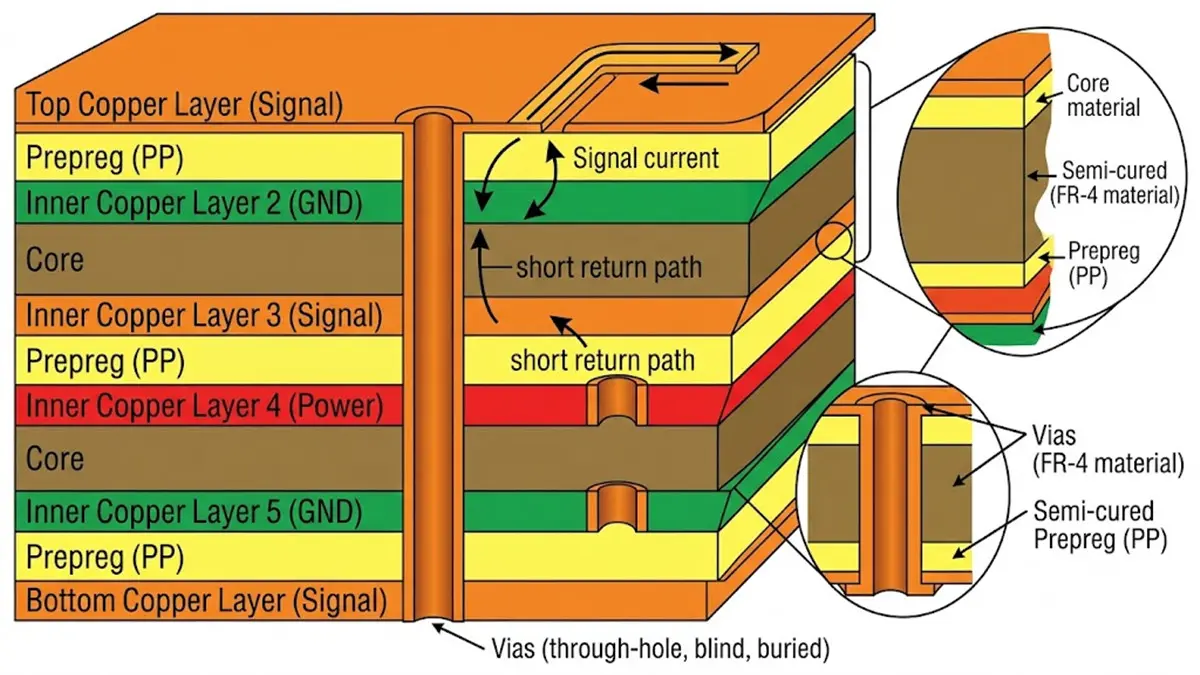
Typical 6-Layer High-Precision PCB Stackup Structure and Signal Return Path Diagram
- 2-Layer Board (Low-Speed Configuration): Signal layer directly references the bottom ground layer. It lacks intermediate shielding and can only satisfy low-frequency or ultra-short trace control.
- 4-Layer Board (Standard Configuration): Composed of
Top (Signal) - Inner 1 (GND) - Inner 2 (Power) - Bottom (Signal). This is the classic industry standard where both Top and Bottom layers have excellent adjacent reference planes, resulting in very short impedance return paths. - 6-Layer and Higher Boards (High-End Configuration): Integrates multiple dedicated GND layers to achieve cross-isolation between signal layers. Multiple ground layers absorb high-frequency radiation, which is widely utilized in 5G core networks and high-speed servers.
4.3 Engineering Difficulties in Mixed Impedance Design
Modern PCBs often accommodate single-ended signals (such as 50Ω clock lines) and differential signals (such as 90Ω USB, 100Ω Ethernet, or PCIe) on a single board. During design, independent impedance modeling and layer routing planning must be performed for each specific group of networks. Special attention must be paid to controlling mutual coupling effects (crosstalk) between different pairs to prevent adjacent high-speed traces from degrading each other’s impedance references.
5. Core Manufacturing Processes: Micro-Level Control
The manufacturing phase translates design blueprints into physical reality. Every process step represents a microscopic battle to protect the target impedance line.
5.1 Detailed Explanation of Five Core Processes
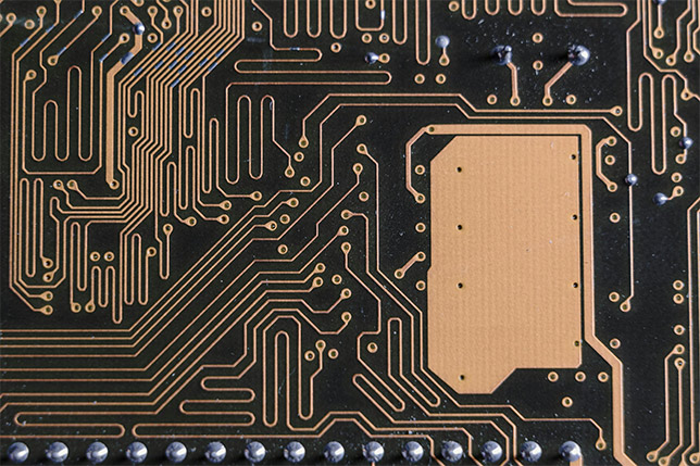
- Etching Control: Because chemical etchants spray downward, the top of the trace is exposed to the chemical longer than the bottom, inevitably causing side etching. This results in a “trapezoidal” trace cross-section. Manufacturing plants must implement an etching compensation mechanism (artificially widening the trace width during the photo-plotting stage to offset side etching), ensuring that the final physical trace width error is strictly controlled within ±0.02 mm.
- Lamination Precision: Multilayer boards are bonded together under high temperature and pressure using prepreg (PP). Improper pressure or temperature curves can lead to excessive resin flow or uneven distribution, directly causing sudden changes in dielectric thickness H. Modern factories generally use vacuum hydraulic presses to reduce layer misalignment to an absolute minimum.
- Back-drilling Process: When high-speed signals transition layers through a via, a section of the copper barrel that carries no current is left behind in the unused layers, known as a Stub. This stub acts as a parallel capacitor, causing severe signal reflections and impedance resonance at high frequencies. Utilizing depth-controlled back-drilling technology to drill out this excess stub (typically retaining <0.2 mm) eliminates the source of reflection and maintains impedance continuity.
- Solder Mask Ink: Solder mask inks typically have a Dk between 3.5 and 4.0. When applied over a surface microstrip line, it effectively increases the dielectric constant on the air side, dropping the single-ended impedance by 2Ω to 5Ω. Therefore, the thickness of the solder mask over impedance traces must be highly uniform. In ultra-high-frequency circuits, traces are often left exposed (solder mask opening) to avoid this effect.
- Surface Treatment:
- ENIG (Electroless Nickel Immersion Gold): Provides an extremely flat surface that facilitates the soldering of fine-pitch components, making it the preferred choice for high-end, high-speed boards.
- HASL (Hot Air Solder Leveling): Due to the unevenness of the air knife blowing mechanism, the solder surface can become irregular and varying in thickness. At high frequencies, this induces severe impedance disturbances, so it is recommended only for low-cost, conventional products.
5.2 Closed-Loop Solutions for Manufacturing Defects
- Resin Smear: Often caused by high drilling temperatures melting the resin, which then coats the hole wall and compromises subsequent copper plating. The solution involves optimizing the lamination process resin ratio and curing time, alongside introducing plasma desmearing after drilling.
- Layer Misalignment: Poor alignment of multilayer boards. The mandatory introduction of CCD automatic optical alignment systems keeps the mechanical alignment error between inner cores and outer layers during lamination within microscopic bounds.
6. Impedance Testing, Quality Control, and Inspection Specifications
Once manufacturing is complete, strict quantitative metrics must verify that the impedance complies with all requirements.
6.1 Technical Division between TDR and VNA
- TDR (Time Domain Reflectometer): Works by launching a fast-rise-time step pulse signal into the transmission line while monitoring the reflected waveform. Based on the time and amplitude of the reflected wave, the TDR instantaneously plots the impedance curve versus distance (impedance profile). It pinpoints exactly where an impedance discontinuity occurs (such as at a via or etching defect), serving as the core diagnostic tool for 100% production line testing.
- VNA (Vector Network Analyzer): Operates in the frequency domain, primarily measuring the S-parameters (such as S11 reflection, S21 loss) of the transmission line through frequency sweeping. While its precision is extremely high, its operation is complex and its testing cost is elevated, making it ideal for material verification during laboratory development, simulation model calibration, and high-end product spot-checking.
6.2 IPC-6012 Inspection Standards and Sampling Strategies
Based on the product’s operating lifecycle and failure consequences, the IPC-6012 standard implements graded management for impedance tolerances:
- General Consumer Electronics (e.g., household appliances): Impedance tolerances are typically relaxed to ±10%, and a 5%-10% batch sampling strategy is used to balance cost and yield.
- High-Reliability Systems (e.g., industrial control, automotive, servers, medical monitoring, military, and aerospace): Impedance tolerances must be tightened to ±5% or ±3% and 100% full inspection is strictly enforced (typically measured via dedicated impedance coupons designed on the PCB panel border).
To guarantee TDR data accuracy, the testing environment must feature adequate metal shielding to isolate spatial RF noise, and the TDR probes must undergo rigorous Short-Open-Load (SOL) calibration with standard components prior to testing.
7. Technology Deployment across Cutting-Edge Application Scenarios
Different industries place distinct emphasis on PCB impedance control, highlighting different engineering priorities:
- Smart Automotive Electronics: Operates in harsh environments with severe vibrations and high temperatures exceeding 125°C. Its impedance tolerance must be within ±3%, mandatory High-Tg materials and low thermal expansion processes must be utilized, and the entire flow must pass the vehicle-board exclusive AEC-Q200 reliability certification.
- 5G/6G Communication Infrastructure: Basestation antennas and high-frequency backplanes handle massive data throughput. These designs demand a “differential-impedance-prioritized” approach. Beyond controlling impedance, managing dielectric loss (Df) via specialized low-loss materials is critical, requiring stringent control over Dk fluctuations across wide frequency bands.
- High-Precision Medical Equipment: Applications like MRI signal acquisition boards or implantable electronic devices tolerate zero data errors. Impedance control implements full-link traceability and 100% microscopic cross-section inspections, striving for “zero defects” and extreme long-term physical stability.
- Aerospace and Military Electronics: Must withstand intense radiation, hard vacuums, and extreme temperature fluctuations in space. Their PCBs incorporate premium military-grade substrates, and production processes target ultra-high-precision limits, prioritizing maximum environmental endurance over commercial cost.
Expert-Level Frequently Asked Questions (FAQ)
Why must automotive and medical electronics pursue an ultra-narrow ±3% impedance tolerance?
In conventional consumer electronics, signal speeds are lower, and the reflection noise from a ±10% tolerance usually does not reach the chip’s noise margin. However, in automotive electronics (such as autonomous driving LiDAR or millimeter-wave radar) and core medical sampling equipment, signals operate at ultra-high frequencies where human life is directly impacted. An impedance deviation of even 5% can induce wave distortions that cause radar to misjudge obstacle distances or cause medical equipment to miss critical physiological waveforms. Therefore, the most stringent ±3% control must be enforced.
Beyond removing the via stub, what collateral benefits does back-drilling bring?
The core purpose of back-drilling is resolving impedance discontinuities. Its secondary benefits are substantial: first, it significantly reduces the parasitic capacitance of the via, greatly improving the insertion loss of high-speed signals through the transition; second, removing the unutilized stub substantially lowers electromagnetic crosstalk between adjacent vias, indirectly purifying the entire PCB’s EMI environment.
In high-speed digital circuits, does ENIG completely outperform HASL across all dimensions?
For high-speed electrical performance and physical flatness, ENIG absolutely outperforms HASL. Because HASL leaves an uneven surface finish, high-frequency signals experience substantial conductor loss and phase shifting due to the skin effect traveling over irregular geometries. However, ENIG contains an underlying layer of nickel (Ni). Nickel is a ferromagnetic material, and in high-power RF fields (such as the output stages of high-frequency power amplifiers), the nickel layer can introduce unwanted non-linear distortion, known as Passive Intermodulation (PIM). Consequently, in specific pure RF/microwave high-power circuits, engineers avoid ENIG in favor of nickel-free finishes like Immersion Silver or Immersion Tin. In low-frequency, highly price-sensitive mixed-signal boards, HASL maintains a major market share due to its low cost and mature processing.
Conclusion and Industry Outlook
PCB impedance control is an interdisciplinary systems engineering challenge spanning material physics, microwave electromagnetics, mechanical processing, and statistical quality control. From initial stack-up simulation modeling to production-line chemical etching, vacuum lamination, precise back-drilling, and final TDR inspection, a failure in any single link will cause the entire impedance control effort to collapse. As modern electronics advance toward 112Gbps/224Gbps PAM4 and even higher high-speed standards, future impedance control will no longer rely solely on simplistic trace width and thickness adjustments. Instead, it will accelerate toward more microscopic and three-dimensional optimizations, such as fiber-weave effect mitigation (optimizing fiberglass cloth alignment), copper foil micro-topography engineering, and fully 3D matched via impedance structures. Firmly adhering to IPC standards and thoroughly understanding the physical mechanisms behind every parameter remains a mandatory core discipline for every outstanding electronic engineer.
About Author
David Chen https://www.linkedin.com/in/pcbcoming
David Chen boasts an extensive professional background in PCBA manufacturing, PCBA testing, and PCBA optimization, with specialized expertise in high-precision PCBA fault analysis and rigorous PCBA reliability testing. The author has worked with high-layer-count server PCB fabrication, ultra-low-loss backplane stackups, and thermo-mechanical reliability optimization for AI infrastructure projects involving 112G and 224G PAM4 architectures. Skilled in complex circuit design and cutting-edge advanced PCB manufacturing processes, he delivers solutions that elevate product durability and performance across industrial applications. His technical articles focusing on PCBA manufacturing workflows and testing methodologies are widely cited by industry peers, research institutions, and technical platforms, solidifying his reputation as a recognized technical authority in the global circuit board manufacturing sector.