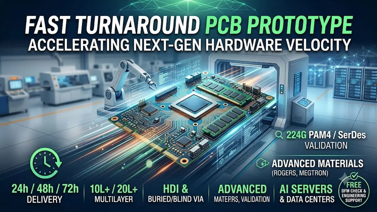
As the core component supporting high-speed signal transmission in advanced electronics, High Frequency PCB (HF PCB) is the cornerstone of innovation in AI, 5G-A, autonomous driving, and satellite communication. In 2026, HF PCB breaks through traditional bottlenecks, moving towards higher integration, lower loss, and greener development. Below is a key point summary of its core segments.
- Definition of High Frequency PCB
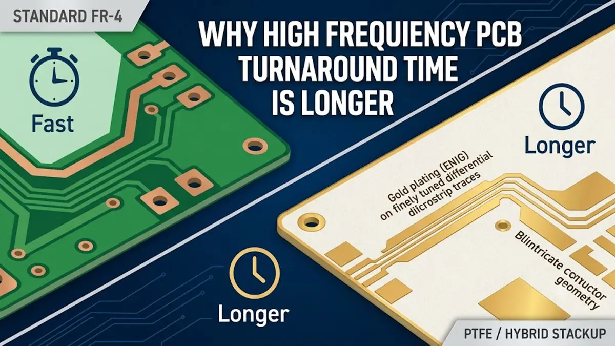
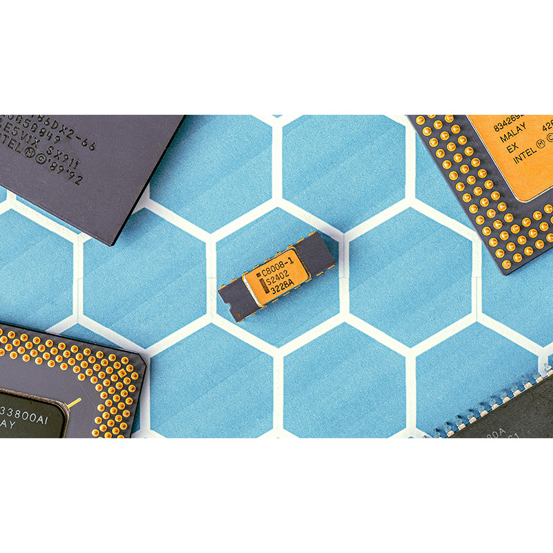
- Basic Definition: A special PCB designed for stable signal transmission at frequencies above 1GHz, different from conventional FR-4 PCBs.
- Core Focus: Minimize signal attenuation and electromagnetic interference (EMI), maintain precise impedance control.
- Key Technical Indicators: Low dielectric constant (Dk: 2.2–3.5), low dissipation factor (Df: ≤0.0015), impedance consistency (±5% fluctuation for 50Ω/75Ω), excellent thermal/dimensional stability.
- Technical Applications of High Frequency PCB (2026 Focus)
- 5G-A & 6G Pre-research: Used in Massive MIMO antennas, base station RF units, and 6G terahertz communication prototypes (frequencies ≥3.5GHz).
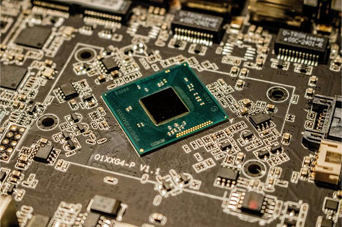
- AI & High-Speed Computing: Applied in GPU motherboards, ultra-high-layer backplanes for AI servers (e.g., Nvidia Rubin platform, Google TPUv7, Huawei Ascend 950), adapting to high-bandwidth, low-latency demands.
- Autonomous Driving: Core for 77GHz millimeter-wave radar (ADAS systems) and lidar, growing with L4-level autonomous driving popularization.
- Satellite Communication & Optoelectronics: Used in satellite-borne systems (lightweight, radiation-resistant) and 400G/800G optical modules (CPO, OCS systems).
- Technical Advantages of High Frequency PCB
- Ultra-Low Signal Loss: Adopts low-loss materials (PTFE, Q cloth) to reduce attenuation, Df as low as 0.001.
- Precise Impedance Control: Avoids signal reflection/crosstalk via advanced design, critical for high-integration equipment.
- Excellent Environmental Adaptability: High Tg (≥280℃), good thermal stability and moisture resistance, suitable for extreme environments (aerospace, automotive).
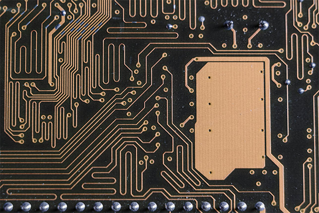
- High Integration Potential: Combines HDI technology (line width/spacing ≤20μm), reduces product volume while integrating more functions.
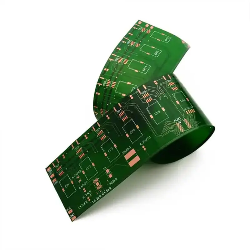
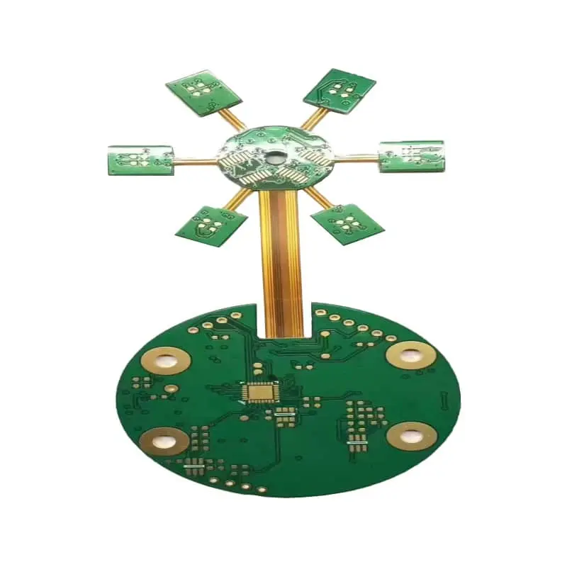
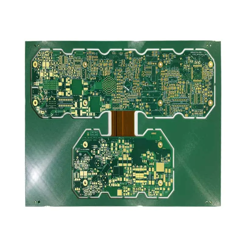
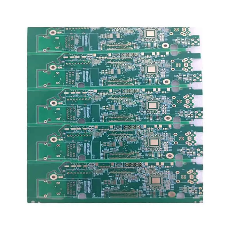
- Multilayer High Frequency PCB Applications
- Core Advantage: Saves space, integrates functions, reduces signal interference, mainstream in high-end fields in 2026.
- AI Server Backplanes: 70-layer+ Midplane/orthogonal backplanes (mass production preparation), interlayer error ≤±5μm, 40-80 layers for mainstream AI servers.
- High-End Communication: 16-32 layer HF PCB integrates RF, power, and control modules for 5G-A base stations and satellite equipment.
- Automotive Electronics: 8-16 layer HF PCB for on-board radar and intelligent cockpits (adapts to limited space and high reliability demands).
- Materials for High Frequency PCB (2026 Innovations)
- Core Base Materials: Traditional (PTFE, Rogers RO4350B/RO4003C) + M9-grade CCL (integrates high-frequency resin, HVLP copper foil, Q cloth) for Rubin platforms.
- Key Auxiliary Materials: Q cloth (Dk: 2.2–2.3, 25-30% supply gap in 2026); HVLP-4/5 copper foil (domestic substitution breakthrough); hydrocarbon resin (67% of M9 formula).
- Emerging Materials: Glass substrate (next-gen packaging, lab-to-industrial verification in 2026); environmentally friendly modified epoxy resin.
- Manufacturing Capabilities of High Frequency PCB (2026)
- Core Processes: Precision etching (line width/spacing control ±10%); laser drilling (solves PTFE drilling issues); plasma/chemical roughening (enhances PTFE bonding); AI-driven impedance control/quality inspection.
- Capacity Layout: 300 billion yuan global high-end supply gap; leading manufacturers expand capacity (high-layer, HDI-integrated HF PCB); Southeast Asia AI PCB industrial cluster formed.
- Technical Barriers: High barriers in material processing, process control, quality testing; integrated “R&D-design-manufacturing” enterprises have competitive advantages.
- 2026 Trends & Innovations of High Frequency PCB
- AI-Empowered Design & Manufacturing: Reduces R&D cycles by 30%, improves yield by 15% (electromagnetic simulation, intelligent inspection).
- Material System Innovation: M9-grade materials become mainstream; domestic substitution accelerates (Q cloth, HVLP copper foil); low-loss, low-cost new materials R&D focus.
- Ultra-High Layer & High-Density Integration: 100-layer+ products enter market; integration with Chiplet technology improves efficiency.
- Green & Low-Carbon Development: Environmentally friendly materials (non-brominated flame retardants) and energy-saving processes, full-life-cycle green production.
- Emerging Application Expansion: Penetrates quantum computing, wearable medical devices, UAVs (supports quantum signal transmission).
Conclusion
In 2026, HF PCB enters a high-end, intelligent, green development cycle, with expanding applications and accelerating domestic substitution. Grasping these trends helps enterprises seize market opportunities and promote industry high-quality development.