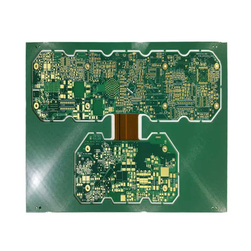
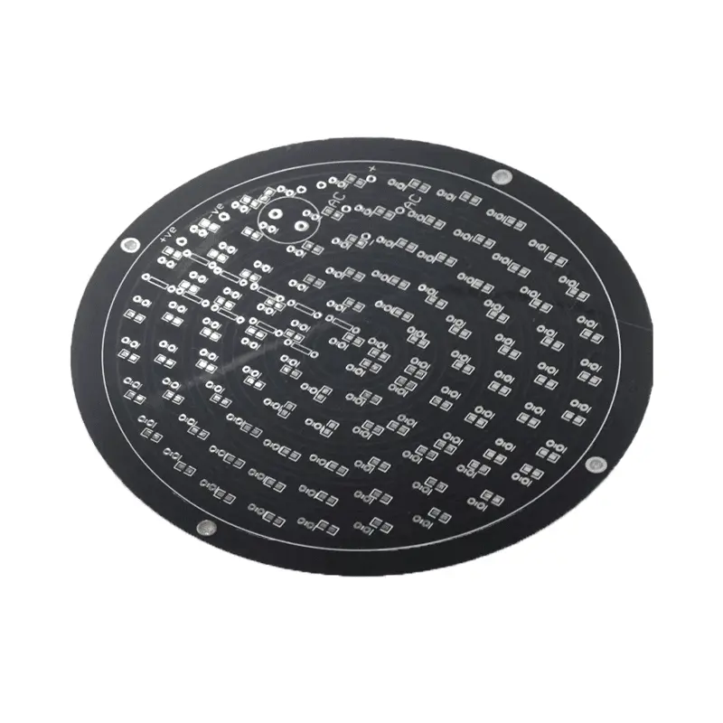
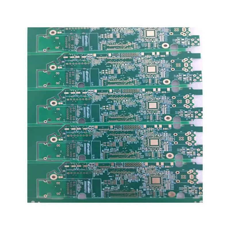
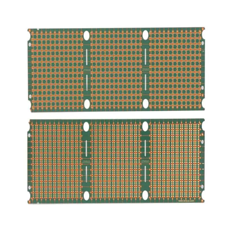
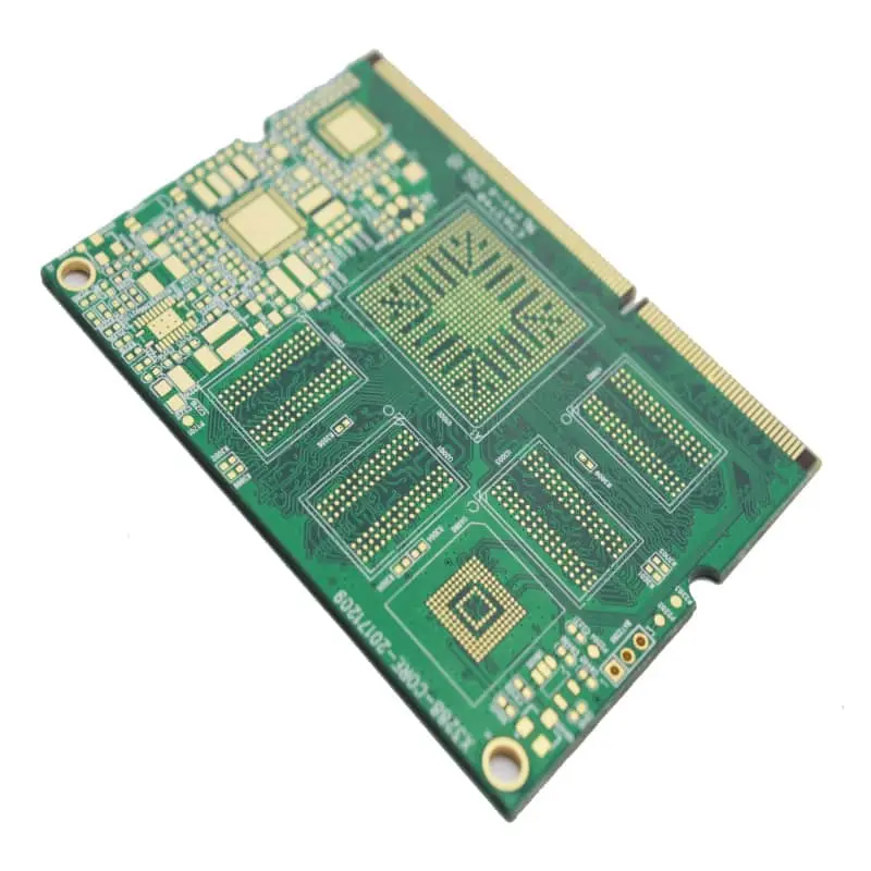
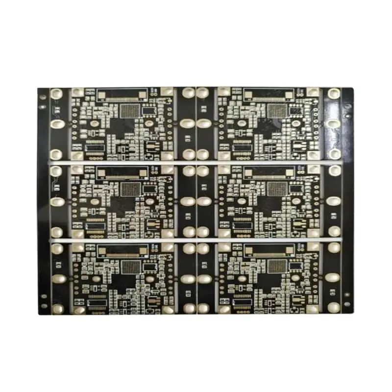
RF PCB Manufacturing serve as the physical foundation for radar, satellite communications, automotive radar, aerospace, and wireless telecom hardware. Many engineering teams treat RF performance as fully locked‑in at design completion, yet real‑world insertion loss, return‑loss degradation, and impedance drift frequently originate from manufacturing variability. Successful RF PCB delivery depends not only on schematic and layout work, but on tightly controlled fabrication workflows, informed material trade‑offs, verified impedance validation, and disciplined supplier selection. This article breaks down actionable, quantifiable process knowledge for electrical, procurement, and quality engineers working on high‑reliability RF hardware.
RF vs. Standard PCB Fabrication: Where the Process Window Actually Shrinks
Standard FR‑4 PCB manufacturing targets cost‑effective volume production with comparatively broad acceptable tolerances. RF and microwave PCBs narrow these windows dramatically, because minor physical deviations directly alter signal‑integrity metrics at GHz frequencies. The table below contrasts key production parameters, with values referenced against IPC‑6012 for rigid PCBs and IPC‑6018 for high‑frequency microwave boards, widely adopted by US defense, aerospace, and automotive radar programs IPC china
| Parameter | Standard PCB (IPC‑6012 Class 2) | RF / Microwave PCB (IPC‑6018) |
|---|---|---|
| Trace‑width tolerance | ±1.0 mil (±25.4 μm) | ±0.5 mil (±12.7 μm), down to ±0.2 mil (±5 μm) for mmWave |
| Dielectric‑layer thickness tolerance | ±10 % | ±3–5 % of nominal thickness |
| Impedance tolerance | ±10 % typical | ±5 % standard; ±3 % for high‑performance mmWave systems |
| Copper‑foil roughness | Standard‑profile copper | Low‑profile (LP) / very‑low‑profile (VLP) copper for reduced skin‑effect loss |
| Surface‑finish insertion‑loss allowance | Loss rarely evaluated | Nickel‑containing finishes create measurable additional conductor loss above 10 GHz |
| Yield driver | Short/open defects | Impedance shift, insertion‑loss drift, dimensional variation |
Design simulation assumes ideal rectangular traces, uniform dielectric thickness, and consistent copper surface quality. Every fabrication step can erode these ideal conditions: excessive side‑etch, laminate thickness swing, copper roughness, and surface‑finish material properties accumulate to degrade RF behaviour. RF performance is therefore continuously shaped throughout manufacturing rather than fixed at layout sign‑off, which makes granular process awareness essential before releasing designs for fabrication.
The Step‑by‑Step Fabrication Flow and the RF Tolerances That Ride on Each Step
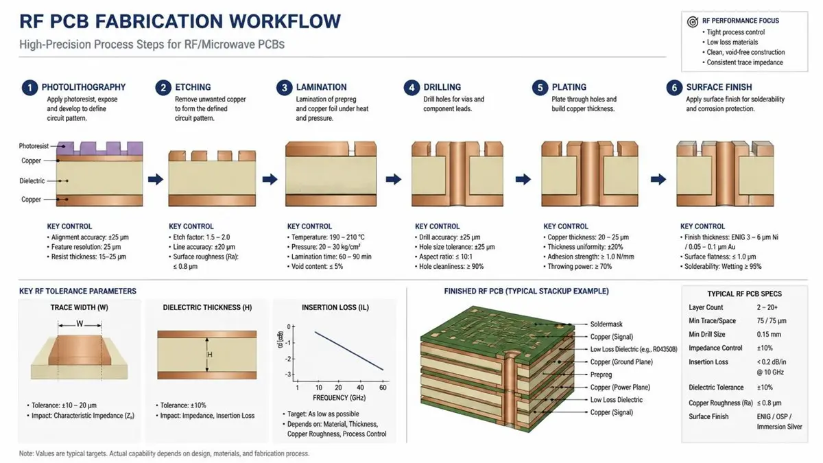
Key RF PCB fabrication workflow, showing how process deviations impact critical high‑frequency tolerance performance
Each core manufacturing operation introduces specific deviation modes that change RF electrical characteristics. Understanding the chain “process deviation → RF consequence → acceptable control range” enables productive technical conversations with your PCB fabricator, rather than relying on vague high‑level requirements.
- Imaging & photolithography: Poor exposure alignment causes trace‑width distortion. Mis‑imaging shifts trace geometry, moving impedance outside target windows. Registration tolerances of ±2–3 mil are baseline for multi‑layer RF hardware.
- Etch and side‑etch control: Lateral side‑etch under resist creates trapezoidal trace cross‑sections instead of ideal rectangles. Additional side‑etch of 0.2–0.4 mil changes characteristic impedance by multiple ohms, worsening return loss. Fabricators must apply trace‑width compensation calculated for the selected copper weight and etch chemistry.
- Lamination: Press temperature‑pressure profiles drive dielectric thickness and effective Dk drift. Hybrid stackups mixing PTFE, hydrocarbon‑ceramic, and epoxy materials require custom lamination cycles. Layer‑to‑layer registration error misaligns signal traces relative to reference ground planes, distorting impedance and increasing coupling.
- Drilling and back‑drilling: PTH hole wall quality, resin smear, and un‑removed via stubs raise insertion loss. For mmWave hardware, back‑drill stub lengths are commonly limited to ≤3–5 mil (75–125 μm) to minimise resonant‑mode degradation. PTFE materials require specialised drill parameters to avoid smearing and delamination.
- Plating: Non‑uniform copper thickness across panels and within barrel walls shifts transmission‑line geometry. Plating thickness variation must be bounded to keep impedance within specification limits.
- Surface‑finish selection: ENIG and ENEPIG include low‑conductivity nickel layers that add substantial insertion loss above 10 GHz. Immersion silver delivers lower RF loss but brings tarnish‑handling constraints; OSP offers near‑copper baseline loss with shorter shelf‑life. Engineers must select finish based on operating frequency, assembly requirements, and link‑budget margin rather than defaulting to ENIG for all projects.
Low‑ and ultra‑low‑profile copper foils used for RF impose modified desmear and oxide‑treatment procedures. Units are frequently specified in both mil and micrometres for cross‑border US engineering workflows, eliminating unit‑conversion miscommunication.
Material Selection and Layer Stackup: The Trade‑offs Nobody Quantifies
Material selection cannot rely solely on datasheet Dk and Df values. Real‑world decisions balance dielectric performance, coefficient of thermal expansion (CTE), moisture absorption, thermal conductivity, copper‑foil grade, component cost, minimum order quantities, lead‑time risk, and alternate‑material pathways during supply‑chain constraints.
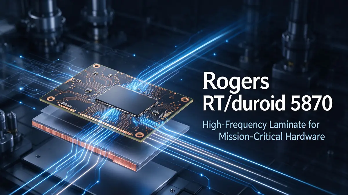
- PTFE‑based laminates deliver ultra‑low loss for millimetre‑wave radar and satellite hardware but carry higher cost, longer lead‑times, and specialised drilling and lamination requirements.
- Hydrocarbon‑ceramic substrates provide competitive high‑frequency performance with processing behaviour closer to modified epoxy.
- Hybrid‑pressure (hybrid‑stackup) constructions place expensive high‑frequency material only on critical RF signal layers, while using conventional lower‑cost dielectrics for non‑RF inner layers to contain total board cost.
Stack‑up design extends beyond dielectric selection. Ground‑plane continuity, return‑path routing, and via‑fence stitching spacing directly control crosstalk and isolation. The most overlooked procedural step is formal stack‑up sign‑off: submit the complete stack‑up drawing, exact dielectric part numbers, copper‑foil specifications, and impedance targets to your manufacturer for written confirmation before production artwork release. Many RF board failures trace back to skipping this formal review step.
Impedance Control, Test Coupons, and Validation: Proving the Board Actually Works
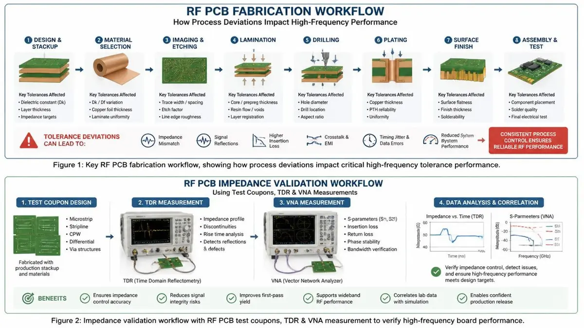
Impedance validation workflow with RF PCB test coupons, TDR & VNA measurement to verify high‑frequency board performance.
Impedance error accumulates from multiple independent sources: trace‑width etch deviation, dielectric‑thickness fluctuation, copper‑thickness non‑uniformity, and soldermask thickness variation. Satisfying each individual parameter in isolation does not guarantee final impedance compliance, as tolerances stack statistically.
Two primary impedance‑tolerance classes dominate RF work: ±5 % for most controlled‑impedance RF circuits and ±7 % for less‑demanding cost‑sensitive applications. Define your requirement explicitly in fabrication notes. Test‑coupon design largely determines whether measured data reflects real‑product performance: coupons must replicate signal‑layer pairs, dielectric thickness, copper type, and transmission‑line geometry found on functional circuit areas. Place coupons at multiple panel locations to capture panel‑wide process gradients, and document defined sampling frequency before production starts.
Match your test equipment to what you need to validate:
- TDR (Time‑Domain Reflectometry): Measures static impedance profiles from test coupons for conformance against impedance targets.
- VNA (Vector Network Analyser): Characterises insertion loss and return loss (S‑parameters) across operating frequency bands.
- Flying‑probe / flying‑point test: Validates continuity and DC resistance; cannot verify RF performance.
- X‑ray and microsection analysis: Investigates hole‑wall integrity, layer registration, lamination voids, and serves as root‑cause failure‑analysis evidence.
Collect test records tied to lot numbers. When yield anomalies appear, coupon and microsection data feed back to adjust etch compensation or lamination cycles to tighten future production distributions.
Optimization Priorities: Yield, Cpk, Scrap, and Choosing a Fab Partner Who Can Hold the Process
Optimising RF PCB manufacturing means translating abstract quality goals into measurable KPIs: process‑capability index (Cpk), first‑pass yield, scrap rate, panel‑utilisation efficiency, and manufacturing lead‑time. Conflicting trade‑offs are common. For example, adjusting panel layout to improve panel utilisation can alter copper‑thickness distribution across the panel, worsening impedance spread.
As a practical illustration, after tuning etch compensation and lamination profiles, one RF production run saw impedance values cluster much closer to nominal targets, scrap percentage reduced, and Cpk metrics improved. Quantitative before‑and‑after metrics carry far more weight than descriptive marketing claims.
Evaluating RF‑capable fabricators goes beyond equipment checklists. Request objective process‑performance evidence: historical Cpk data for impedance, experience processing your specific high‑frequency laminate families, and confirmation that production follows IPC‑6018 acceptance grades. For US‑bound defence‑aerospace projects, confirm applicable compliance certifications and traceability workflows.
Cost drivers differ between low‑volume prototypes and high‑volume production runs. Layer count, selected high‑frequency laminate, surface finish type, and tight tolerance requirements dominate pricing. High‑frequency‑material supply volatility frequently extends lead‑times, so pre‑quotation material‑availability checks reduce project delays.
Use this practical supplier‑audit checklist as part of your RF‑PCB sourcing workflow:
- Can you provide Cpk statistics for impedance on comparable RF stack‑ups?
- Do you hold stock or established supply channels for my specified RF laminates?
- Will you formally review and sign‑off my complete stack‑up before manufacturing release?
- What coupon layout and sampling plan will you implement for this order?
- Which IPC acceptance class will govern inspection and acceptance criteria?
Take Action for Your Next RF PCB Project
Avoid costly spins and un‑explained RF performance gaps by leveraging our RF‑focused engineering support:
- Send your stack‑up drawings and impedance targets for a free design‑for‑manufacturability review.
- Download our editable RF fabrication‑notes template and supplier‑evaluation checklist for your next RFQ cycle.
- Book a technical consultation call with our RF process engineers; non‑disclosure agreements are available. We offer US‑aligned engineering support and fast RF‑PCB prototyping turnaround. Submit your request today to receive feedback within one business day.
Frequently Asked Questions
What makes RF PCB manufacturing different from standard PCB fabrication?
RF PCBs require far tighter dimensional and material‑property tolerances. Minor deviations in trace geometry, dielectric thickness, copper roughness, and surface finish directly degrade GHz‑range insertion loss and impedance performance, whereas those same deviations are acceptable for conventional digital‑signal hardware. IPC‑6018 defines dedicated requirements for microwave‑grade boards, compared to IPC‑6012 for general rigid PCBsIPC中国.
What impedance tolerance should I specify for a high‑frequency board, and how is it verified?
±5 % impedance tolerance is typical for most RF hardware; mmWave systems may require ±3 %. Validation relies on properly designed test coupons measured via TDR, with supplementary VNA testing to check insertion‑loss and return‑loss S‑parameters. Generic continuity testing cannot validate RF impedance compliance.
Which surface finish is best for low‑loss RF PCBs: ENIG, ENEPIG, or immersion silver?
Immersion silver delivers the lowest insertion loss among these three options, though it carries tarnish‑risk and limited shelf‑life. ENIG and ENEPIG incorporate lossy nickel barrier layers that degrade high‑frequency performance, despite offering excellent solderability and long shelf‑life. OSP achieves near‑copper loss but is not suitable for wire‑bonding applications.
How much does copper‑foil roughness affect insertion loss at millimetre‑wave frequencies?
At mmWave frequencies, skin depth shrinks, forcing signal energy to travel very close to the copper surface. Higher surface roughness increases effective conductor loss significantly. That is why VLP / HVLP ultra‑smooth copper foils are standard for 28 GHz and higher designs.
What should I include in the fabrication notes and stack‑up sign‑off for an RF board?
Include full stack‑up construction, exact laminate part‑numbers, copper‑foil type for each signal layer, explicit impedance targets and tolerance limits, test‑coupon requirements, back‑drill stub‑length limits, surface‑finish specification, and the governing IPC acceptance class. Obtain written manufacturer confirmation before releasing artwork.
How do I reduce scrap and improve yield on high‑frequency PCB builds?
Complete formal stack‑up sign‑off, define proper coupon geometry and sampling, require Cpk‑based process‑control evidence from your fabricator, select realistic tolerances aligned with actual system margin, and perform microsection failure analysis on non‑conforming units to drive iterative process improvements.
What drives cost and lead‑time for low‑volume RF PCB prototypes made in the United States?
Specialised high‑frequency‑laminate material availability, low‑order‑quantity surcharges, tight tolerance requirements, selected surface finish, layer‑count complexity, and mandatory test and documentation for aerospace‑defence‑grade hardware all shape pricing and lead‑time timelines.
About Author
David Chen LinkedIn Profile
David Chen is a Senior RF/PCB Process Engineer at Shenzhen Hongda Circuit Technology Co., Ltd., with over 12 years of experience in high-frequency PCB fabrication, impedance-controlled stack-up design, and Rogers/PTFE laminate processing. He also boasts an extensive professional background in PCBA manufacturing, PCBA testing, and PCBA optimization, with specialized expertise in high-precision PCBA fault analysis and rigorous PCBA reliability testing. The author has worked with high-layer-count server PCB fabrication, ultra-low-loss backplane stackups, and thermo-mechanical reliability optimization for AI infrastructure projects involving 112G and 224G PAM4 architectures. Skilled in complex circuit design and cutting-edge advanced PCB manufacturing processes, he delivers solutions that elevate product durability and performance across industrial applications. His technical articles focusing on PCBA manufacturing workflows and testing methodologies are widely cited by industry peers and technical platforms, and have gained attention and recognition from industry colleagues.