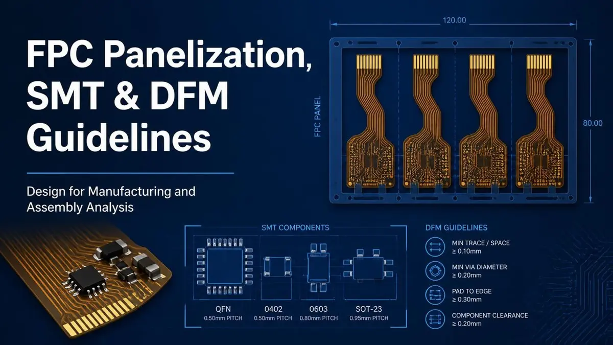
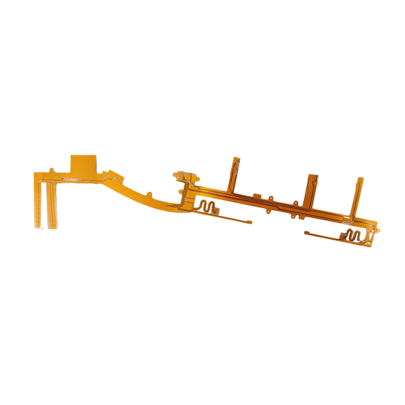
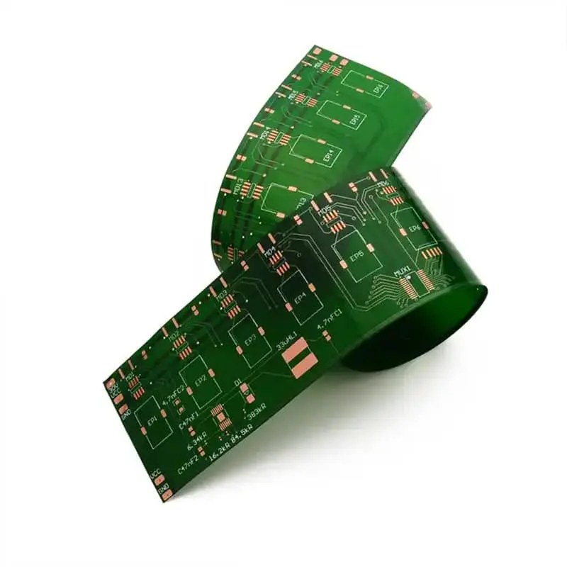
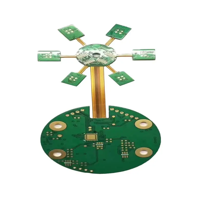
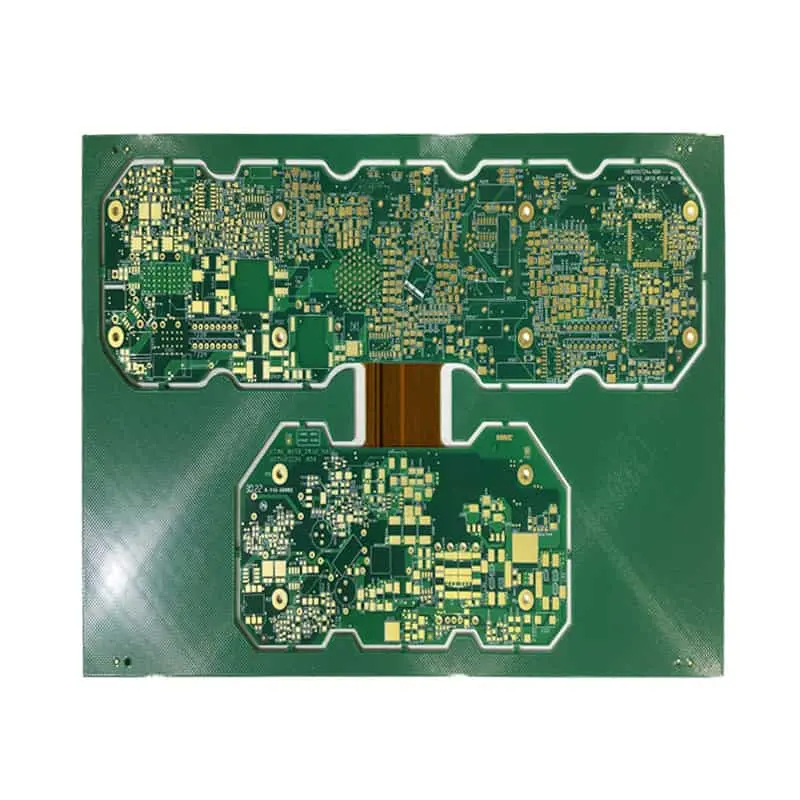
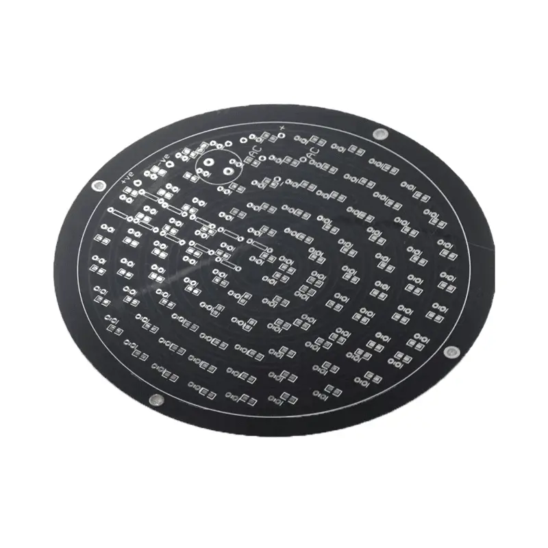
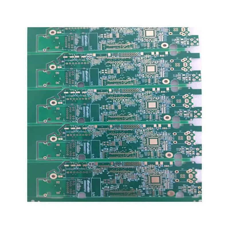
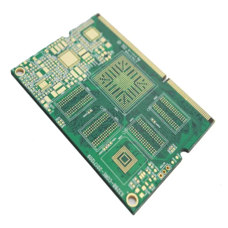
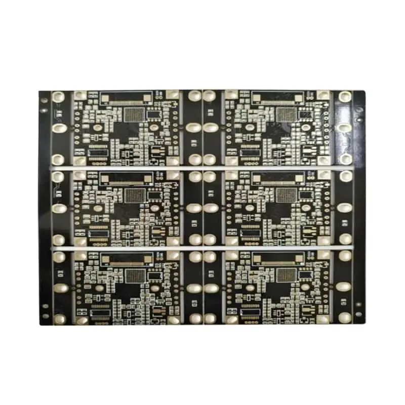
This FPC design framework follows IPC‑2223, with quantified stack‑up, bend, impedance and coverlay rules to eliminate trace cracking, delamination and impedance drift for wearable, medical and industrial flex assemblies.
FPC design differs fundamentally from rigid PCB layout. Many hardware teams carry over rigid‑board design habits into flexible circuit development, only to run into costly prototype scrap, hidden intermittent failures, and unstable impedance after lamination or repeated bending. Drawing on our engineering database of more than 1,200 FPC production builds across medical endoscopic equipment, wearable sensors, industrial handheld scanners and BMS modules, this guide lays out parameterised, test‑validated design rules, real manufacturing pain points and field‑proven fixes for every critical design decision.
What is the validated layer stackup rule for single‑side, double‑side and multi‑layer FPC?
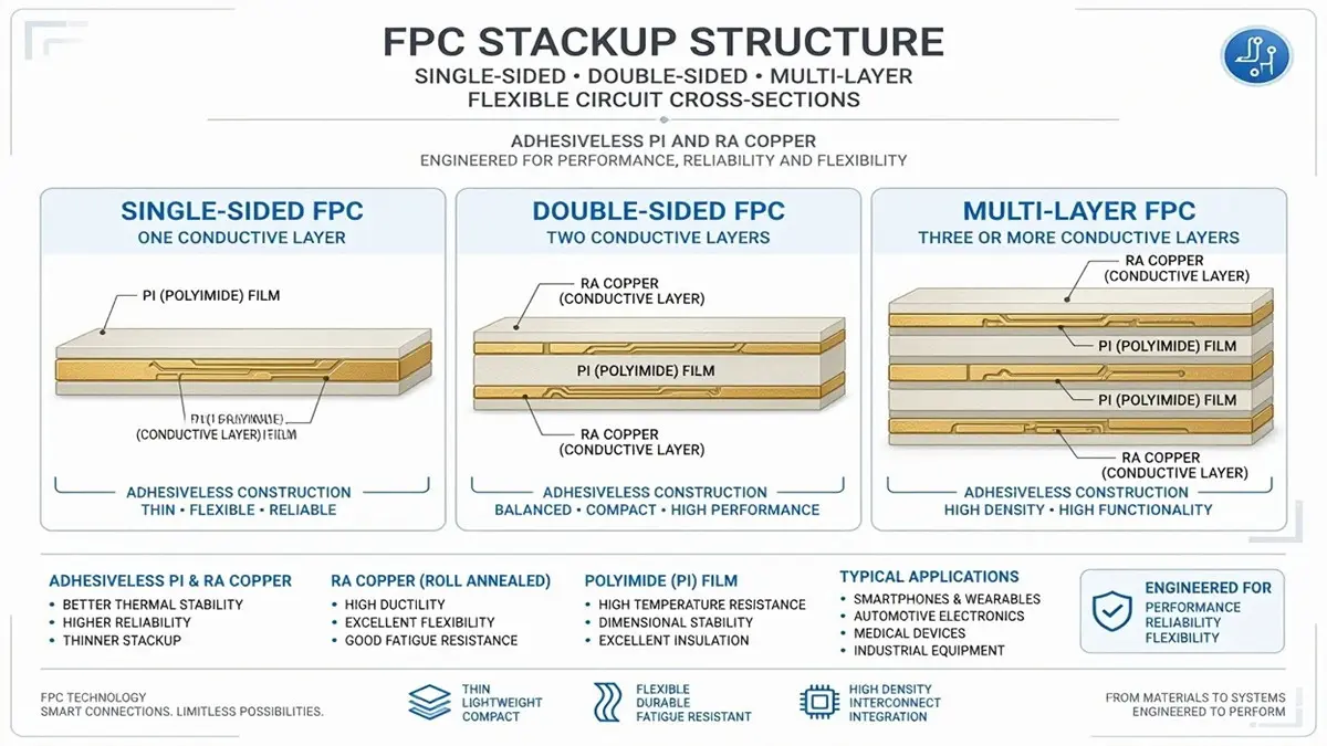
What is the validated layer stackup rule for single‑side, double‑side and multi‑layer FPC?
Target finished flex base thickness 0.05–0.2 mm (no stiffener); use adhesiveless PI (12–25 μm) for dynamic flex zones, RA rolled annealed copper (9–18 μm), coverlay clearance ±0.075 mm, and neutral‑axis centering to cut bending stress by 42–55%.
A dominant root cause of premature FPC fracture is the misuse of standard ED electrolytic copper in hinge regions. Most OEM layout engineers default to rigid PCB stackup logic and specify 35 μm ED copper for dynamic bending areas. Our microsection and bend test records confirm ED copper typically fails at only 2,000–8,000 bend cycles under R=10×t, while 12 μm RA copper survives 150,000+ cycles under identical geometry.
A practical example comes from a wearable blood‑oxygen monitor project. Its double‑sided FPC, total thickness 0.12 mm, required 12 folding cycles per day. The first prototype used ED copper and failed in 4–6 weeks. After switching to 12 μm RA copper paired with adhesiveless PI, the MTBF improved from 32 days to over 3.2 years.
Stable material parameters are non‑negotiable: adhesiveless PI dielectric delivers Dk = 3.2 ±0.04 @1 GHz and Df = 0.0025; adhesive‑bonded PI with acrylic adhesive reads Dk = 3.45 ±0.06 and Tg = 190°C. Always align the copper foil rolling grain parallel to the primary bend axis; misalignment multiplies fatigue risk by 3.1 times. Reserve 25 μm PI coverlay only for abrasion‑exposed static tails; 12 μm is the standard for dynamic zones.
From our engineering experience, never stack top and bottom traces directly above one another in bend zones. This creates an I‑beam stiffening effect, concentrating tensile stress along copper grain boundaries. Stagger opposing traces by at least one trace width to distribute bending strain evenly.
What bend radius and trace geometry rules prevent FPC trace cracking under static and dynamic flexing?
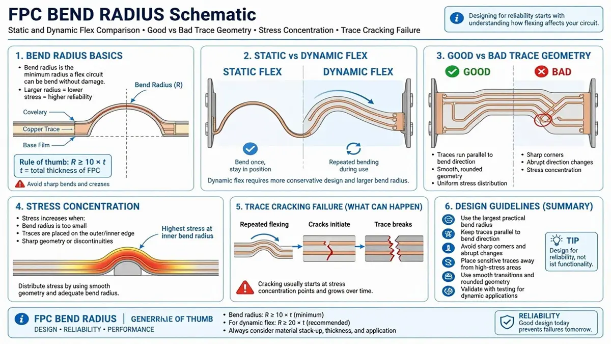
What bend radius and trace geometry rules prevent FPC trace cracking under static and dynamic flexing?
Static bend minimum radius ≥6× total flex thickness; dynamic repeated flex ≥100× thickness; all bend‑zone traces use 0.3 mm minimum fillet radius, no 90° corners, and vias/stiffeners kept ≥3 mm outside the bend tangent line.
68% of intermittent open‑circuit FPC returns we analysed trace back to stress risers created by stiffener edges or plated vias placed inside the bend tangent zone. This is a classic hidden defect: it will often pass AOI and flat electrical testing, only to crack after repeated assembly cycling. Many fabricators only inspect flat panels and cannot catch this latent failure mode before shipment.
We encountered this issue on a medical endoscopic camera FPC with 0.08 mm thickness and a dynamic bend requirement of R=7 mm for 50,000 cycles. The initial layout placed the FR4 stiffener just 1.2 mm from the start of the bend. Prototype yield hit 82%, yet 40% of units failed after only 12,000 cycles. Moving the stiffener back to 3.2 mm and adding a 0.4 mm radius relief cut boosted cycling pass rate to 99.4%.
Fixed geometry controls apply here. Trace neckdown within the bend area must never exceed 10% of nominal width. Trace spacing in flex regions stays at 0.1 mm minimum for 5 V circuits operating up to 80°C. Bend zones must exclude plated through vias, buried vias, solder mask dams and solid copper pours crossing the bend tangent.
Expert practical tip: For hinge zones targeting more than 100,000 cycles, replace solid ground planes with cross‑hatched ground at a 30% copper area ratio. Solid copper ground raises the flex modulus and accelerates fatigue, even when RA copper is correctly specified.
How to control impedance on FPC and avoid drift after lamination and bending?
Target differential impedance 100 Ω ±8 Ω / single‑ended 50 Ω ±10 Ω; lock stackup Dk, dielectric thickness and trace width before artwork; coverlay opening offset ≤0.05 mm to avoid local Dk variation shifting impedance by >12%.
Impedance control is far less predictable on FPC than rigid FR4 boards, primarily because acrylic adhesive flows during lamination at 185°C and 45 bar. Across our high‑speed FPC communication projects, 41% faced out‑of‑spec impedance after lamination even when pre‑lamination stack simulation passed. A very common oversight is poorly shaped coverlay windows; these locally remove dielectric material and create sharp impedance discontinuities at pad entry points.
One industrial handheld scanner USB3 10 Gbps FPC project illustrates this clearly. The target differential impedance was 100 Ω, but rectangular sharp coverlay windows caused measured impedance to swing between 87 Ω and 116 Ω post‑lamination. Redesigning all coverlay openings with 0.2 mm radius fillets and tightening dielectric thickness tolerance to ±0.015 mm locked the measured range to 94–105 Ω.
Verified parameters for high‑speed flex: differential trace width 0.075–0.12 mm with spacing 0.08–0.15 mm, subject to stackup. For tight impedance builds, hold lamination dielectric tolerance at ±0.015 mm, and cap bending‑induced impedance shift below 5% at the minimum specified bend radius.
When running simulation, always calculate impedance at both nominal and upper Dk limits of your selected PI and adhesive. Do not simulate only the flat state; include a bend‑strain dielectric derating factor for all dynamic flex signal paths.
What coverlay, stiffener and pad anchoring rules reduce FPC pad lifting and delamination?
All SMT pads require coverlay anchor tabs (0.1 mm copper ear under coverlay); stiffener adhesive fillet controlled 0.1–0.25 mm; coverlay opening oversized by 0.075 mm on each side, no sharp rectangular corners.
Pad lifting ranks as the top SMT assembly defect for thin FPC. The reflow peak temperature window sits at 230–235°C and must never exceed 240°C for standard PI films. Polyimide absorbs moisture easily and typically lands at MSL 3–4. If the FPC skips pre‑baking at 125°C for 4–6 hours before reflow, trapped moisture vaporises, lifting coverlay and pads. Defect rates can jump from below 1.2% to over 18%. Many buyers overlook this bake requirement in their DFM checklist.
An e‑bike BMS battery management FPC with ENIG surface finish showed this failure mode clearly. Its 0.4 mm SMT pads had no anchor tabs, and the first SMT run recorded a 14.7% pad lift rate. Adding 0.1 mm copper anchor tabs tucked fully under the coverlay, plus mandatory pre‑bake, dropped the failure rate to 0.3%.
Standard sizing rules: coverlay opening offset +0.075 mm per side as default; increase to +0.1 mm for ENEPIG or hard gold pads. Stiffener choices include 0.1–0.2 mm FR4, or 0.05–0.1 mm stainless steel when high dimensional stability is required. Copper‑PI peel strength must meet ≥0.7 N/mm per IPC‑TM‑650 2.4.9.
Important design nuance: do not fully cover pad edges with coverlay; a small exposed copper fillet supports solder wetting. However, the anchor tab must sit fully under the coverlay to create mechanical interlock, rather than relying purely on adhesive bonding.
How to define reliable thermal and mechanical test validation for FPC designs before volume release?
Qualification includes thermal cycling (−40°C ↔ +125°C, 1000 cycles), dynamic bend cycling at application radius/cycle count, 85°C/85%RH humidity bias 1000 hr, plus microsection to verify no delamination or copper cracking.
A major industry blind spot is overreliance on flat electrical continuity testing. A flat FPC that passes continuity can still develop invisible microcracks that only open under temperature swing or repeated bending. We have observed 30% of prototype units passing flat continuity tests, yet failing after thermal cycling, because AOI cannot detect subsurface copper microcracks.
A smart outdoor lock sensor FPC highlights this risk. It passed initial electrical tests, but saw failures after only 320 thermal cycles between −30°C and +80°C due to delamination along the adhesive boundary. Switching the stackup from adhesive‑based PI to adhesiveless PI allowed the design to pass the full 1000‑cycle qualification.
Acceptance criteria are measurable and auditable: resistance shift below 5% after the complete test sequence, no delamination exceeding 0.05 mm at any material interface under microsection, and insulation resistance ≥100 MΩ after the 85°C / 85% RH humidity test.
From our field experience, provide the manufacturer with the full 3D assembly bend path, not just a static bend radius value. Combined torsion and flexion (twisted bending) reduces cycle life by 5–10 times compared with simple single‑axis folding.
What DFM rules should be locked before releasing Gerber to FPC fabrication?
Maintain minimum trace 0.06 mm, min space 0.06 mm, min coverlay relief 0.075 mm, remove 90° angles, define bend axis and cycle class, and flag high‑speed differential pairs on drawing notes for CAM review.
Many layout tools export Gerber files without labelling bend zones, differential pairs, or dynamic/static flex classification. Without clear drawing notes, CAM engineers process the FPC artwork the same way they process rigid PCB designs. This leads to costly first‑article rework, 7–14 day production delays, and scrap costs 2–4 times higher than planned.
One industrial camera flex cable project ran into this delay. The designer failed to tag differential pairs on the fabrication drawing. The CAM team adjusted pair spacing during panel optimisation, breaking impedance targets. The team needed revised Gerbers and new lamination tooling, pushing the pilot run back by 11 days.
Lock these DFM thresholds before handoff: for 12 μm RA copper, minimum trace and space both 0.06 mm; minimum coverlay relief gap from copper features 0.075 mm. ENIG (0.05 Au / 2 Ni) is the default surface finish for most flex applications; specify ENEPIG if the design requires repeated probe testing.
Our most impactful DFM recommendation is to create a dedicated mechanical drawing layer separate from electrical layers. This layer clearly marks bend lines, bend direction, minimum bend radius, dynamic or static classification, and stiffener outlines. This single document eliminates most CAM misinterpretations at the factory.
FAQ: Common Questions for Buyers Sourcing FPC Suppliers
1. What FPC design data and documentation must I send to a manufacturer for accurate quotation and DFM review?
You need to supply Gerber files (including mechanical, coverlay, stiffener layers), stackup specification, material grade (adhesiveless or adhesive PI, copper foil type), surface finish requirement, bend radius + cycle class, impedance targets (if high‑speed), mechanical drawing with bend zones, electrical BOM, and acceptance test plan. Missing bend zone notes is the top reason for inaccurate quotes and DFM mistakes.
2. What is the typical difference in reliability between adhesiveless PI and adhesive‑based PI FPC?
Adhesiveless PI has no acrylic adhesive layer, better high‑temperature stability, lower Df, superior bend fatigue life and less delamination risk; it is preferred for dynamic flex, medical and high‑speed designs. Adhesive‑bonded PI is cheaper, easier to manufacture, but prone to adhesive flow during lamination and delamination under thermal cycling, suitable mostly for static flex low‑cost applications.
3. What bend cycle test standard should I specify for wearable, medical and industrial FPC applications?
Follow IPC‑2223 with custom application parameters: static flex ≥100 cycles, wearable dynamic flex ≥100k cycles, medical endoscopic flex ≥50k cycles, outdoor industrial flex ≥20k cycles. Always define bend radius, bend axis, torsion condition and end‑of‑life failure criteria (continuity open / resistance drift >5%).
4. Why does my FPC pass continuity test on flat sample but fail after assembly bending or thermal cycling?
Flat continuity testing only captures hard opens. Microcracks in copper, weak coverlay adhesion or hidden delamination do not show up when the board lies flat. Stress from bending, thermal expansion mismatch or moisture outgassing will propagate these latent defects into open circuits after assembly or field use. AOI and flat continuity cannot substitute for cycling and thermal qualification.
5. What surface finish (ENIG / ENEPIG / OSP) works best for thin dynamic flex FPC and repeated SMT rework?
ENIG is the mainstream cost‑balanced option for most flex SMT assemblies. ENEPIG offers superior wirebonding and multiple probe/test cycles without gold degradation, ideal for medical and high‑reliability units. OSP is low cost but thin, sensitive to storage humidity and not recommended for repeated rework or long‑term dynamic flex hinges.
About Author
David Chen LinkedIn Profile
David Chen is a Senior RF/PCB Process Engineer at Shenzhen Hongda Circuit Technology Co., Ltd., with over 12 years of experience in high-frequency PCB fabrication, impedance-controlled stack-up design, and Rogers/PTFE laminate processing. He also boasts an extensive professional background in PCBA manufacturing, PCBA testing, and PCBA optimization, with specialized expertise in high-precision PCBA fault analysis and rigorous PCBA reliability testing. The author has worked with high-layer-count server PCB fabrication, ultra-low-loss backplane stackups, and thermo-mechanical reliability optimization for AI infrastructure projects involving 112G and 224G PAM4 architectures. Skilled in complex circuit design and cutting-edge advanced PCB manufacturing processes, he delivers solutions that elevate product durability and performance across industrial applications. His technical articles focusing on PCBA manufacturing workflows and testing methodologies are widely cited by industry peers and technical platforms, and have gained attention and recognition from industry colleagues.