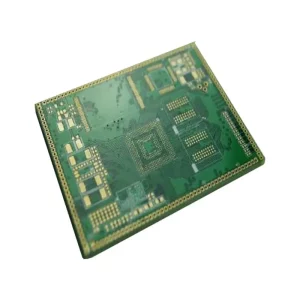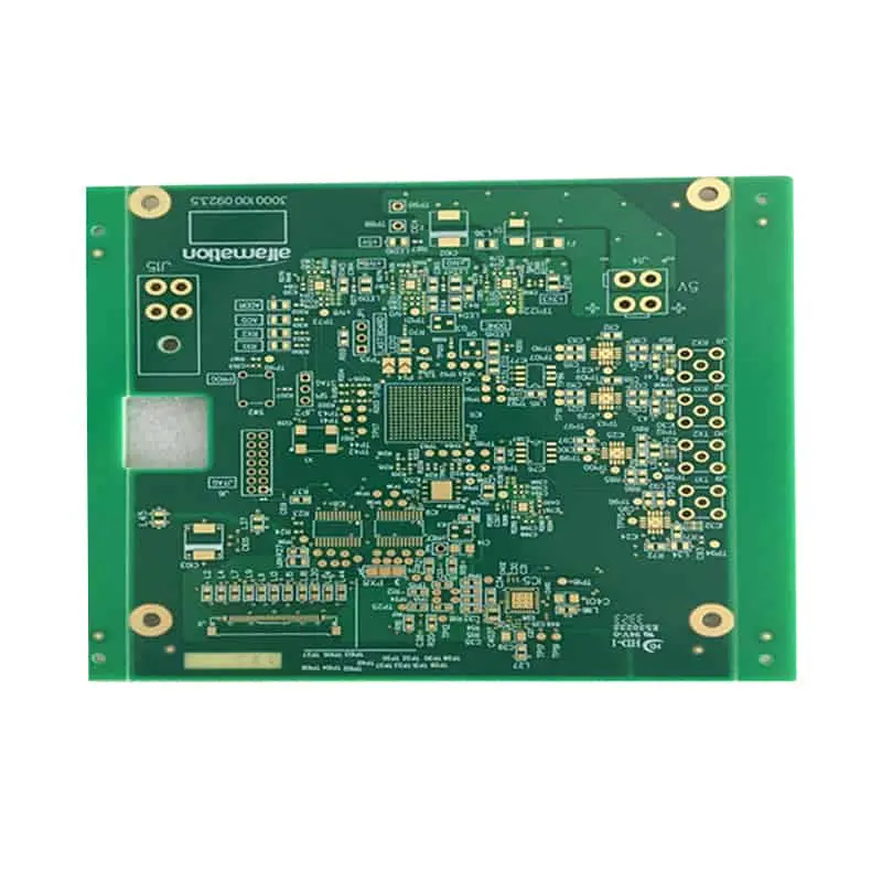
10 Layer ENIG PCB
The advantage of the gold immersion process is that when printing the line, the color on the surface is very stable, the brightness is very good, the plating is very flat, and the weldability is very good.The thickness of gold immersion is generally 1-3 Uinch, so the gold thickness made by this appearance treatment of gold is generally thicker, so the appearance treatment of gold is widely used in key boards, gold finger boards and other circuit boards, due to the strong conductivity of gold, good oxidation resistance, long service life.
Share to:
| Key attributes |
| Industry-specific attributes |
| Number of Layers:10-layer |
| Base Material:TG170(FR4) |
| Board Thickness:1.6mm |
| Board Size:OEM |
| Other attributes |
| Model Number:Wonderful PCB&PCBA |
| Type:Multilayer pcb |
| Copper Thickness:1OZ |
| Min. Hole Size:0.1mm |
| Min. Line Width:0.075mm |
| Min. Line Spacing:0.075mm |
| Surface Finishing:OSP, BGA,,impedance,resin plugging |
| Solder Mask Color:green, blue, black, red, yellow |
| Standard Certification: ROHS, ISO14001, UL, ISO9001-2000 |
| Surface treatment:Hasl lead free, flash gold, gold finger, immersion silver |
| Sample order:sample order acceptable |
| Service available:OEM acceptable, PCB Assembly available |
| PCB Test:Flying probe test, e-test fixture, visual inspection |
| Profiling punching:V-cut, rounting, beveling |
| Specialized in:high-precision, high-density double-sided pcbs, multilayer pcb |
| Shipping:Sea, air shipment, express courier |
| Packaging and delivery |
| Package Type: |
| Inner package: Vacuum package. Outer package:Carton package |
| attribute-list |
| Supply Ability:50000 Square Meter/Square Meters per Month. |