
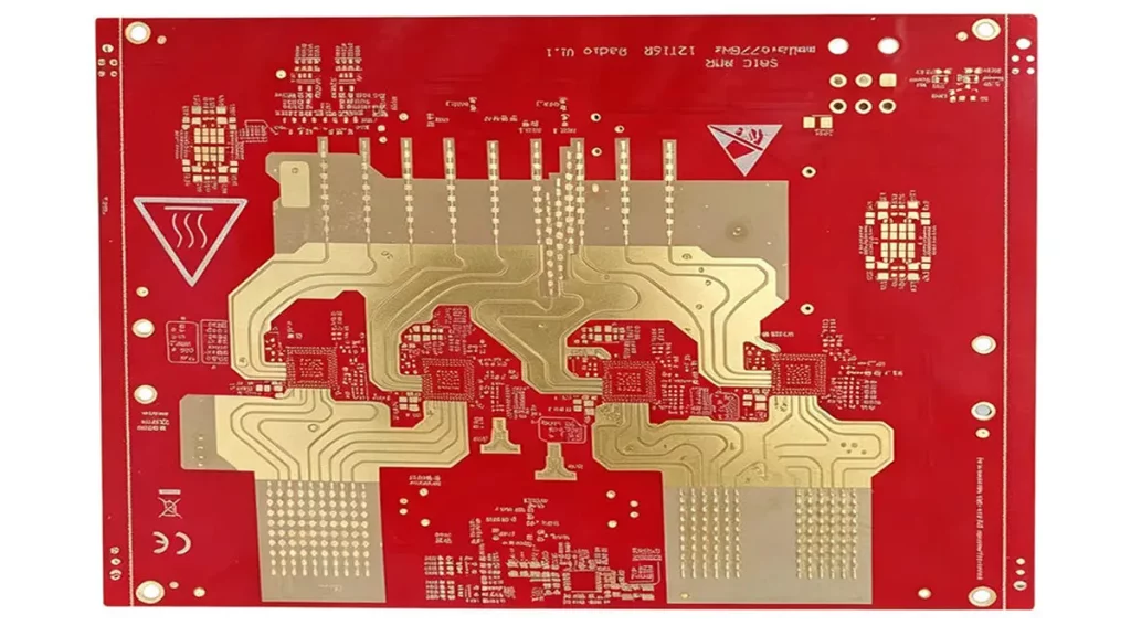
High Frequency Communication PCB Manufacturer for Blind & Buried Holes Printed Circuit Board and PCBA Assembly
High frequency communication PCBs require controlled impedance, low-loss materials, short RF transitions, stable grounding, and tightly controlled fabrication. For 2.4 to 6 GHz wireless systems and higher-frequency microwave designs, the PCB stackup, copper geometry, dielectric properties, via structure, and connector transition must be engineered together rather than specified independently. For OEMs and RF engineers sourcing […]
