Low-temperature co-fired ceramic
(LTCC) PCBs have become the substrate of choice for RF/microwave modules, aerospace electronics, and high-density packaging where FR-4 falls short and conventional high-temperature ceramics are too costly or too difficult to integrate. This guide covers the technology, materials, design rules, and supplier considerations you need to source LTCC boards with confidence.
What Is LTCC PCB? Technology Overview and Core Materials
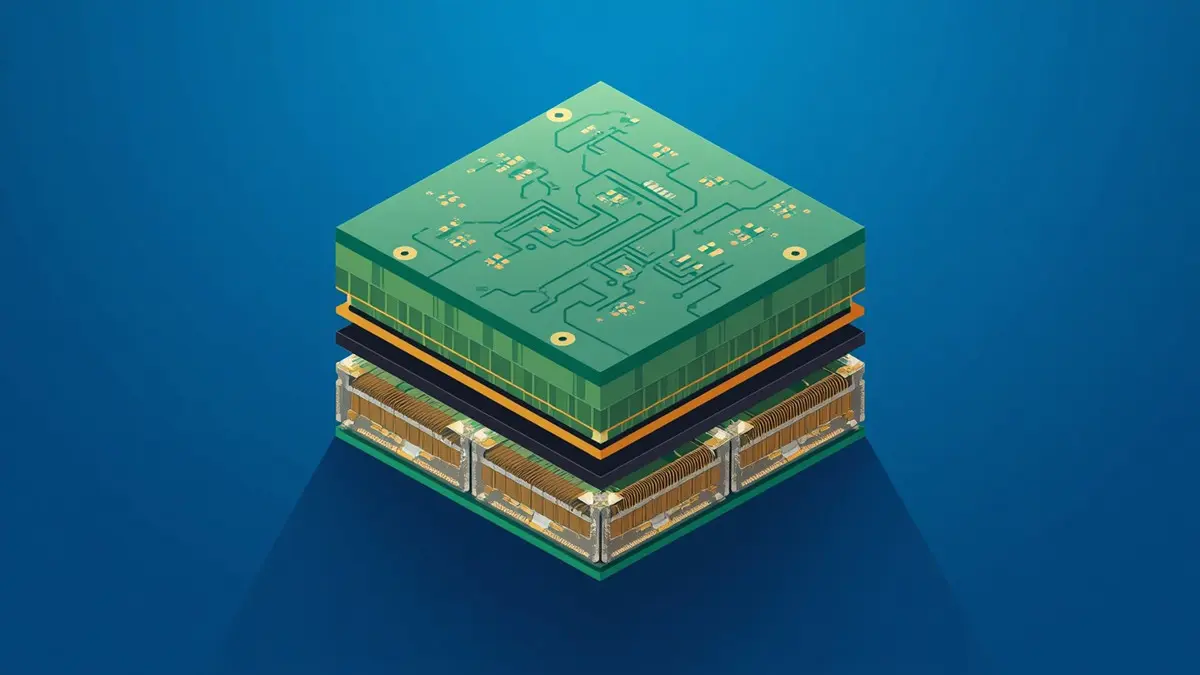
LTCC PCB Multilayer Substrate Structure
An LTCC board is a multilayer ceramic substrate built by stacking unfired “green tape” layers of glass-ceramic dielectric, printing conductor traces and embedded passives on each layer, then laminating and co-firing the entire stack in a single step. Typical formulations include:
Glass-ceramic matrix: Systems such as DuPont’s 9K/951 (εr ≈ 7.8), Heraeus’s Heratape (εr ≈ 5.9), and Ferro’s A6M (εr ≈ 5.9). Higher-εr formulations (εr ≈ 20–80) exist for compact passives.
Embedded passive materials: Printable resistive inks (e.g., RuO₂-based pastes, 1 Ω–1 MΩ/sq) and dielectric pastes for embedded capacitors.
Conductor inks: Silver (Ag), gold (Au), platinum (Pt), and copper (Cu) pastes for signal layers, vias, and terminations, typically screen-printed at 10–20 µm thickness.
Unlike FR-4 (organic laminate), high-frequency ceramic boards (HTCC/BeO), or insulated metal substrates (IMS), LTCC is co-fired with printed conductors and buried vias in one process, creating a true three-dimensional circuit with embedded resistors, capacitors, and inductors. Few materials explain why: the glass phase (often borosilicate or lead-based, though lead-free systems are standard now) softens and densifies below 900 °C, which lets it co-fire with low-resistivity metals like Ag and Cu that would melt or oxidize under HTCC’s 1,500+ °C sintering. This combination of low-temperature sinterability and conductor compatibility is what enables embedded passives at practical cost.
Electrical and Thermal Properties, RF/Microwave Performance, and Thermal Limits
LTCC PCB RF and Thermal Performance Metrics
Key engineering parameters for common LTCC systems:
| Parameter | Typical Range | Notes |
|---|
| Dielectric constant (εr) | 5.9–8.0 (standard); up to 80 (high-εr) | Extremely stable vs. frequency and temperature (Δεr < 1% from –55 to +125 °C) |
| Loss tangent (tanδ) | 0.001–0.003 up to 40 GHz; ~0.002 at mmWave | Compare with FR-4’s 0.015–0.02 — critical for insertion loss above 10 GHz |
| Thermal conductivity | 2–5 W/m·K | 3–10× FR-4, below BeO or AlN (150–200 W/m·K) |
| CTE | 5.8–7.8 ppm/°C | Closely matches Si and GaAs die, improving flip-chip and wire-bond reliability |
Band-by-band implications: At L/S-band (1–3 GHz), tanδ differences are minor, and LTCC wins on integration density. At X-band (8–12 GHz) and beyond, a 0.002 tanδ vs. FR-4’s 0.017 cuts transmission-line loss by roughly 8×, directly enabling smaller filters and antennas. Above 30 GHz, LTCC’s εr stability and smooth copper/gold metallization make impedance control within ±5% routine.
High-temperature operation: Standard LTCC systems operate continuously to 125 °C, with automotive/aerospace-qualified grades rated to 200 °C and short excursions to 400 °C. Primary limits are glass-phase creep under sustained high-temp bias and intermetallic growth at conductor interfaces. Design guidance: use thicker metal (≥15 µm) for power rails, add thermal vias under die, and consider mounting on a Cu/W or Cu/Mo heat spreader for >20 W continuous dissipation.
Fabrication and Co-Firing Process: Shrinkage, Vias, and Metallization Choices
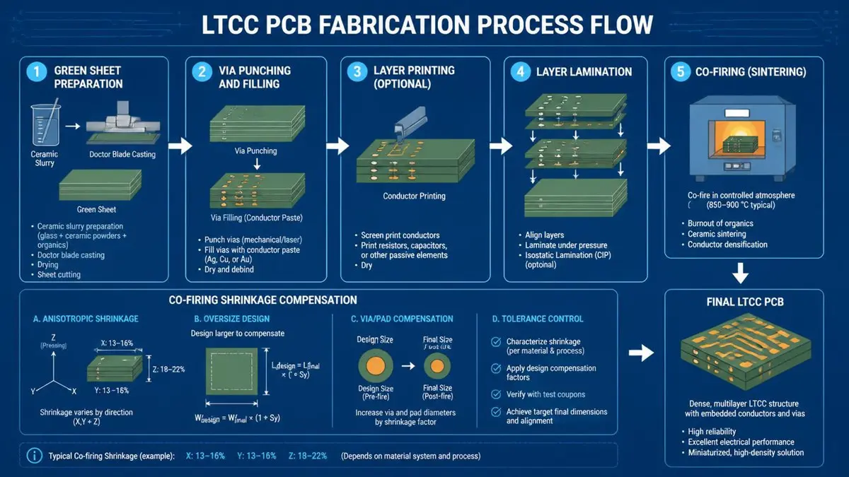
LTCC PCB Fabrication Process and Shrinkage Compensation Flowchart
The LTCC manufacturing flow: green sheet preparation → via punching → via filling and conductor/passive printing → layer inspection → lamination → co-firing → post-firing processing (solder pads, plating, cavity machining).
Shrinkage—the detail competitors skip. Green tape shrinks ~30% linearly (X-Y) and ~45–50% in Z during firing, with system-specific values (e.g., 951: ~12% X-Y with 15% constrained-tape processes; A6M: ~16%). Anisotropy matters: constrained sintering systems (low-CTE setter plates) reduce X-Y shrink to 1–3%, dramatically improving layer-to-layer registration for fine lines. Layout compensation must be applied to every layer’s artwork per the tape vendor’s shrink curves, which vary by lot, print thickness, and lamination pressure.
Via filling options: Silver paste printing (standard, best conductivity, cost-effective for large volumes); via plugging with dielectric paste (for blind vias and planarity); and filled-and-plated vias for high current. Smaller vias (50–100 µm) require higher-viscosity pastes and can trap organics, causing hermeticity failures — specify 100% X-ray inspection on critical designs.
Metallization comparison: Ag is the default (lowest resistivity, lowest cost, best co-fire match but susceptible to electromigration and sulfur corrosion). Au on top of Pt or Pd offers wire-bonding and shelf-life excellence at high cost. Cu delivers the lowest resistance for power and RF but requires nitrogen firing — not all shops offer it. Specify plating (Ni/Au) on I/O pads for solderability and hermetic lid sealing.
Design Rules, Assembly, Soldering Compatibility, and Prototyping Best Practices
Practical design rules for most LTCC vendors (always confirm per supplier):
Min conductor width/spacing: 75 µm/75 µm (production); 50 µm possible in development
Via diameter: 100–200 µm standard; capture pads +50–100 µm; blind via aspect ratio ≤1:1
Layer count: 1–30 layers typical; total thickness 0.3–3 mm after firing
Registration tolerance: ±25 µm per layer cumulative — pad your artwork accordingly
Include a 3–5% layout scale compensation per vendor shrink data, verified on first article
Assembly: LTCC withstands standard lead-free reflow (SAC305, peak 245–260 °C) without damage. Key precautions: use mild or no-clean fluxes (avoid aggressive rosin cleaners on silver-bearing pads), limit rework cycles to 2–3 per pad, and constrain warp to <0.1% over the board for BGA. Ceramic filter, crystal, and RFIC attach with conductive epoxy for RF grounding performance, or eutectic AuSn (80/20) for hermetic high-reliability attach.
Prototyping (U.S. focus): Domestic quick-turn LTCC runs deliver 2–6 weeks for 5–20 layer builds; overseas production can cut unit cost 30–50% at 6–10 week lead times. A hybrid strategy — prototype and qualify domestically, transfer tooling-qualified designs offshore — is standard. Reliability screening should include thermal cycling (–55 to +125 °C, 500 cycles), damp heat (85 °C/85% RH, 1,000 h), and high-temperature storage (200 °C, 1,000 h) per MIL-STD-883 methods.
Applications, Advantages vs. Other Substrates, Costs, Lead Times, and Suppliers
LTCC dominates where RF performance, thermal robustness, and miniaturization converge: satellite transceivers, phased-array radar T/R modules, automotive 77 GHz radar, 5G/6G mmWave front-ends, downhole oil/gas instrumentation, and implantable or space-grade sensor packages.
Trade-off table:
| Criterion | LTCC | FR-4 | High-freq polymer | Thick-copper IMS |
|---|
| mmWave loss | Excellent (tanδ ~0.002) | Poor | Good | N/A (no RF layers) |
| Embedded passives | Yes (R, C, L) | Limited | Limited | No |
| Thermal conductivity | 2–5 W/m·K | 0.3–0.4 | 0.5–1 | 1–3 (base) |
| Size/weight for RF module | Best | — | Good | — |
| Relative cost | High | Low | Medium | Medium |
Budgeting: 4–8 layer prototypes run $500–$2,000 per unit domestically; production pricing drops 10–20× at volume. Lead times: U.S. prototypes 2–6 weeks; offshore production 8–12 weeks. When selecting a supplier, demand: IPC-6011/6018 qualification data, MIL-STD-883 test reports, moisture uptake and CTE mismatch data for their tape system, and shrink-curve documentation for DFM review.
Get Your LTCC Project Started
Ready to move from outline to production? Request sample dielectric data sheets, a free DFM/co-fire compensation review, or a prototype quote today.
Two easy next steps:
Upload your Gerber files and stack-up drawing for a custom co-fire shrink-compensation analysis and manufacturability assessment — typically returned within 3 business days.
Book a 15–30 minute engineering consultation with our applications team to review your thermal, RF, or reliability requirements and available test data. Email:pcb@pcbcoming.com
You can also download our LTCC Designer’s Checklist, a white paper covering shrink compensation, via design, and solder joint reliability — the same document our engineers use for design reviews.
FAQ
What dielectric constant and loss tangent values should I expect for LTCC materials across RF and microwave bands?
Standard systems (DuPont 951, Heraeus Heratape, Ferro A6M) offer εr of 5.9–7.8 with tanδ of 0.001–0.003, stable from LF through 40+ GHz. High-εr pastes (εr 20–80) are available for embedded capacitors but have slightly higher loss.
How much shrinkage occurs during LTCC co-firing and how should I compensate in PCB layout?
Expect 30–50% volumetric shrinkage: roughly 12–16% linear in-plane (or 1–3% with constrained sintering) and 40–50% in thickness. Compensation is applied by scaling artwork per the tape vendor’s shrink curves, verified with a first-article measurement.
Can LTCC boards be assembled with standard SMT reflow processes and which solder alloys are recommended?
Yes — LTCC tolerates standard lead-free reflow (SAC305, peak 260 °C). Use no-clean fluxes, and conductive epoxy or AuSn eutectic for die attach in RF/hermetic applications.
What via filling and metallization options are available for LTCC and how do they affect hermeticity and reliability?
Vias are typically filled with silver paste (best for conductivity and hermeticity when 100% filled), dielectric paste (for blind vias), or left open for conductive epoxy fill. Metal choice (Ag vs. Au vs. Cu) affects corrosion resistance, wire-bondability, and cost.
How do LTCC PCBs compare with FR-4 and other ceramic substrates in cost, thermal performance, and long-term reliability?
LTCC costs 10–50× more than FR-4 per unit at low volume but delivers embedded passives, 10× better thermal conductivity, and MIL-grade reliability (1,000+ hours at 200 °C). Versus HTCC, it allows lower-resistance silver/copper metallization and cheaper firing.
What are typical lead times and prototyping options in the U.S. for LTCC, and how can I shorten time to market?
U.S. prototype lead times are 2–6 weeks for 5–20 layer builds. Shorten time to market by using domestic quick-turn for first articles, pre-qualifying your design against published shrink curves, and transferring to offshore production only after qualification.
About Author
David Chen https://www.linkedin.com/in/pcbcoming
David Chen is a Senior RF/PCB Process Engineer at HAODA ELECTRONIC CO.,LIMITED., with over 12 years of experience in high-frequency PCB fabrication, impedance-controlled stack-up design, and Rogers/PTFE laminate processing. He also boasts an extensive professional background in PCBA manufacturing, PCBA testing, and PCBA optimization, with specialized expertise in high-precision PCBA fault analysis and rigorous PCBA reliability testing. The author has worked with high-layer-count server PCB fabrication, ultra-low-loss backplane stackups, and thermo-mechanical reliability optimization for AI infrastructure projects involving 112G and 224G PAM4 architectures. Skilled in complex circuit design and cutting-edge advanced PCB manufacturing processes, he delivers solutions that elevate product durability and performance across industrial applications. His technical articles focusing on PCBA manufacturing workflows and testing methodologies are widely cited by industry peers and technical platforms, and have gained attention and recognition from industry colleagues.