Multi‑wire PCBs embed discrete pre‑insulated conductive wires inside dielectric substrates to achieve high‑density point‑to‑point interconnections, yet they are frequently mistaken for conventional multilayer PCBs. Engineers turn to multi‑wire PCB technology when standard etched‑trace stack‑ups hit hard limits on routing density, vibration resistance, crosstalk suppression, or excessive layer‑count growth. Many public resources only offer high‑level definitions while omitting practical construction details, critical design‑for‑manufacturing (DFM) rules, real‑world failure risks and actionable selection guidance. This guide breaks down multi‑wire PCB construction, manufacturing constraints, side‑by‑side technology comparisons, industry deployments, performance trade‑offs and clear next steps for your hardware project.
What Is a Multi‑Wire PCB? Definition, Construction, and How the Wiring Layers Work
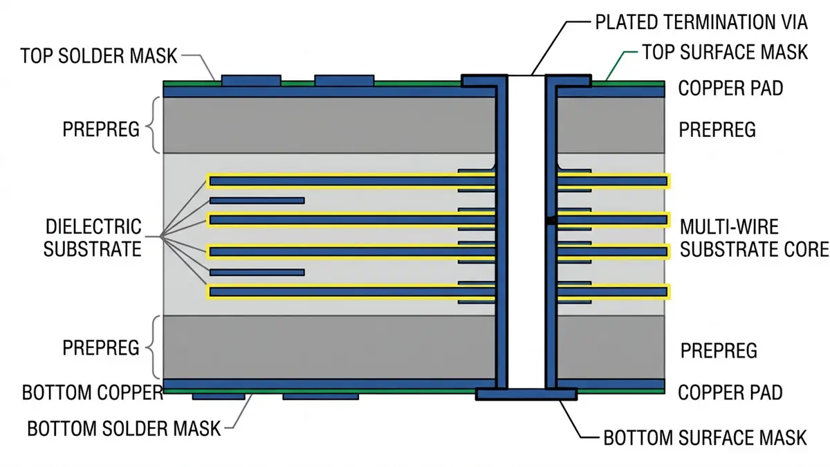
Cross‑section diagram showing embedded insulated wire structure of multi‑wire PCB, demonstrating dielectric layers, embedded conductors and termination vias
A multi‑wire PCB is not an alternative name for standard multilayer PCBs. While traditional multilayer boards form circuits by etching copper foils on stacked laminated layers, multi‑wire PCBs place individual insulated wires within dielectric material to build electrical paths. Interconnections are completed via plated through‑holes, dedicated termination pads or custom contact points rather than continuous etched copper traces.
Key structural building blocks include base dielectric core, individually insulated signal or power wires, bonding prepreg materials for lamination, and termination interfaces linking embedded wires to external circuitry. During production, insulated wires are precisely positioned, secured, and fully embedded under heat‑pressure lamination. Each embedded conductor carries its own insulation jacket, allowing wires to cross one another without short‑circuiting, which directly improves routing density without adding more copper‑etched layers.
Wiring layers inside multi‑wire PCBs operate independently or cooperatively for signal and power distribution. Isolation from surrounding dielectric prevents unintended coupling between adjacent embedded conductors. Compared with conventional multilayer PCBs that must add new physical layers for crossing traces, multi‑wire architectures reduce dependency on stack‑up expansion. To visualize: imagine replacing many fine etched copper traces with insulated miniature wires locked inside board material, connected outward at defined pad and via locations.
No application or cost comparison is covered in this section; understanding physical build forms the foundation for later design and project decisions.
Design, Routing, and Manufacturing: Rules for Embedding, Assembling, and Inspecting Multi‑Wire PCBs
Successful multi‑wire PCB implementation depends on strict design and manufacturing constraints, from initial routing rules through final inspection. Critical layout parameters include wire diameter, minimum wire‑to‑wire clearance, wire bend radius limits, layer‑to‑layer alignment tolerance, termination geometry and transition‑via sizing. Electrical constraints cover controlled impedance targets, crosstalk mitigation, thermal stress thresholds and maximum current‑carrying capacity for embedded conductors.
One commonly overlooked engineering challenge is reliable termination: mechanically and electrically bonding embedded insulated wires to plated‑through‑holes or surface pads. Poor termination is a leading source of field failures, and most competitor documentation skips this critical junction requirement.
High‑level production workflow follows this sequence: precise wire placement → embedding into dielectric → lamination bonding → wire stripping & termination → assembly → electrical test and physical inspection.
Practical Multi‑Wire PCB DFM & Inspection Checklist
- Confirm wire diameter, spacing and minimum bend radius with your fabricator before design freeze
- Validate termination‑to‑plated‑via geometry for mechanical strength and low‑resistance contact
- Document layer‑alignment tolerances for embedded‑wire registration
- Set clear acceptance criteria for lamination voids, referencing relevant IPC class standards for your industry
- Define electrical test coverage for continuity, insulation resistance and impedance verification
- Include post‑assembly visual and non‑destructive inspection steps for termination quality
These rules directly influence manufacturing yield. This section focuses purely on design‑to‑production requirements without covering industry‑specific scenarios or full cross‑technology comparison.
Multi‑Wire PCB vs. Multilayer, HDI, and Rigid‑Flex: Cost, Performance, and Selection Criteria
No single PCB construction fits every project. Selecting between multi‑wire PCB, conventional multilayer, HDI, and rigid‑flex depends on routing density goals, signal‑integrity targets, mechanical operating conditions, budget and expected lead‑time.
| Evaluation Item | Multi‑Wire PCB | Conventional Multilayer PCB | HDI PCB | Rigid‑Flex PCB |
|---|---|---|---|---|
| Routing Density | High; reduces required stack‑up layers | Moderate‑High; density rises by adding layers | Very high via‑driven density | Moderate‑high; combines rigid routing + flex sections |
| Signal Integrity | Strong for point‑to‑point paths; controlled impedance achievable | Excellent with solid reference planes | Excellent for high‑speed miniaturized circuits | Good; pay attention to rigid‑flex transition zones |
| Mechanical / Vibration Performance | Good; embedded wires resist trace cracking | Moderate; etched traces risk cracking under heavy shock | Moderate | Very good; eliminates board‑to‑board connectors |
| Thermal Performance | Depends on wire gauge and dielectric | Excellent with copper power/ground planes | Good | Moderate |
| Relative Prototype Cost | High | Low‑Moderate | Moderate‑High | High |
| Typical Lead‑Time | Longer | Standard | Medium‑Long | Long |
| Manufacturability | Specialized process; limited fabricator pool | Widely available | Broad industry adoption | Specialized fabrication skill required |
Multi‑wire PCB merits consideration for projects experiencing extreme routing congestion, efforts to avoid excessive layer‑count stacking, and systems requiring improved vibration robustness for high‑reliability hardware.
Conventional multilayer, HDI or rigid‑flex architectures deserve evaluation for cost‑sensitive low‑complexity circuits, high‑volume consumer products, and designs requiring physical board bending. Rigid‑flex becomes relevant when dynamic flexing is part of operating conditions.
Note that cost dynamics shift between prototyping and mid‑volume runs. Multi‑wire PCB may become more economically attractive at moderate volumes by cutting total stack‑up complexity. This section avoids deep‑dive industry case studies and focuses entirely on project‑level selection logic.
Industry Applications and Real‑World Use Cases: Aerospace, Defense, Medical, Automotive, and High‑Density Electronics
Multi‑wire PCBs serve demanding vertical markets where standard PCB stack‑ups cannot satisfy mechanical, miniaturization or reliability requirements. Instead of only listing industry names, below are concrete module‑level scenarios.
Aerospace and Defense: Avionics sub‑modules benefit from multi‑wire PCB’s vibration resistance and lightweight construction. In airborne electronics exposed to continuous shock and wide temperature swings, embedded‑wire structures mitigate trace‑cracking risks seen in conventional etched multilayer boards. US aerospace supply‑chain projects prioritize traceable materials and IPC Class‑3 reliability qualifications for these assemblies.
Medical Electronics: Compact diagnostic instruments use multi‑wire PCBs to fit complex wiring inside extremely limited enclosure space while preserving clean signal integrity for low‑noise biometric measurements. Designs must align with medical regulatory expectations for material stability.
Automotive Electronics: Vehicle control modules experience repeated thermal cycling and mechanical vibration. Multi‑wire PCBs deliver stable current‑carrying performance for select safety‑related sub‑circuits where traditional layouts run into routing bottlenecks.
High‑Density Electronics: When multilayer PCB stack‑up grows to impractical layer counts, multi‑wire PCB offers an alternative path to untangle crowded point‑to‑point signal paths without expanding board footprint.
Manufacturing parameters are not repeated here; focus stays on real‑world engineering constraints within each application field.
Performance Benefits, Thermal and EMI Considerations, and Limitations of Multi‑Wire PCBs
Multi‑wire PCB delivers meaningful engineering advantages but also carries well‑defined practical limitations.
Core Performance Benefits
- Higher effective routing density: Insulated crossing wires reduce demand for additional stack‑up layers.
- Improved point‑to‑point signal integrity: Shorter direct conductor paths can lower parasitic inductance and crosstalk in properly configured layouts.
- Enhanced mechanical robustness: Embedded wires offer better resistance against shock‑induced conductor breakage compared to surface‑etched traces.
- Flexible current‑handling: Wire‑gauge selection enables tuning current‑carrying capacity for individual power conductors.
Known Limitations, Risks & Practical Mitigations
- Termination reliability risk: Wire‑to‑via/pad junctions represent potential failure points. Mitigation: strictly follow fabricator termination design rules and include dedicated termination inspection steps.
- Lamination void potential: Trapped air or moisture during lamination creates void defects, which degrade insulation and mechanical stability. Mitigation: control material moisture and specify void acceptance limits per IPC standards.
- Very limited repairability: Once wires are embedded inside dielectric, rework or component‑level trace repair becomes nearly impossible. Mitigation: complete thorough DFM review and prototype validation before full‑scale production.
- Higher design complexity: Special DFM rules differ significantly from standard PCB workflows. Mitigation: involve your manufacturing partner early in schematic and layout phases.
- Cost premium for simple circuits: Multi‑wire PCB is not cost‑effective for low‑complexity designs. Mitigation: run comparative technology evaluation at project kick‑off.
Balanced risk assessment helps hardware teams decide whether multi‑wire architecture is worth adopting for their specific program. This section does not repeat comparison‑table data or full industry case details.
Get Engineering Evaluation for Your Multi‑Wire PCB Project
If your project faces high‑density routing bottlenecks, strict thermal cycling requirements, high‑shock vibration environments or high‑reliability certification targets, request a formal design‑for‑manufacturability review before locking your layout.
Prepare key project information to accelerate assessment: intended stack‑up requirements, wire‑size constraints, signal‑speed and current‑carrying specifications, operating‑temperature range, and required industry certification standards (such as IPC Class‑3 for aerospace). You may submit your design files or requirement worksheet, schedule a technical engineering consultation, or ask for prototype quotation.
We focus on realistic manufacturability, US‑market compliance review and transparent lead‑time estimates without over‑promising performance outcomes. Our engineering team will help you confirm whether multi‑wire PCB, HDI, multilayer or rigid‑flex best fits your program goals.
Frequently Asked Questions
Q: What is a multi‑wire PCB, and what does its basic construction look like?
A: A multi‑wire PCB embeds individually insulated conductive wires within dielectric material, forming point‑to‑point interconnections via pads and plated vias, distinct from copper‑etched multilayer PCBs.
Q: Why do multi‑wire PCBs use multiple wiring layers, and how do those layers work?
A: Separate embedded‑wire layers isolate signal groups; insulated wires can cross without shorts, reducing how many traditional copper‑etched layers you need.
Q: Is a multi‑wire PCB the same as a multi‑wire branch circuit?
A: No. Multi‑wire PCB is a printed‑circuit‑board interconnect technology; multi‑wire branch circuit refers to electrical wiring distribution in building power systems.
Q: When should I choose a multi‑wire PCB instead of a conventional multilayer, HDI, or rigid‑flex board?
A: Multi‑wire PCB fits projects calling for higher routing density and vibration robustness while seeking to avoid an excessively high‑layer‑count stack‑up. Other technologies remain relevant for cost‑sensitive simple circuits or hardware requiring physical flexing.
Q: How are wires embedded, routed, and inspected during multi‑wire PCB manufacturing?
A: Wires are precisely placed, embedded and laminated, then stripped and terminated to vias and pads. Inspection covers termination quality, lamination voids, continuity, impedance and isolation performance.
Q: What are the main limitations, risks, and design constraints of multi‑wire PCBs?
A: Primary risks include termination‑joint reliability, lamination voids, almost‑zero repairability, specialized DFM rules and higher prototype cost.
Q: Do multi‑wire PCBs improve signal integrity, thermal management, and current‑carrying capacity?
A: They can enhance point‑to‑point signal integrity and allow per‑wire current tuning; thermal performance depends heavily on wire gauge, dielectric material and overall stack‑up design.
About Author
David Chen LinkedIn Profile
David Chen is a Senior RF/PCB Process Engineer at Shenzhen Hongda Circuit Technology Co., Ltd., with over 12 years of experience in high-frequency PCB fabrication, impedance-controlled stack-up design, and Rogers/PTFE laminate processing. He also boasts an extensive professional background in PCBA manufacturing, PCBA testing, and PCBA optimization, with specialized expertise in high-precision PCBA fault analysis and rigorous PCBA reliability testing. The author has worked with high-layer-count server PCB fabrication, ultra-low-loss backplane stackups, and thermo-mechanical reliability optimization for AI infrastructure projects involving 112G and 224G PAM4 architectures. Skilled in complex circuit design and cutting-edge advanced PCB manufacturing processes, he delivers solutions that elevate product durability and performance across industrial applications. His technical articles focusing on PCBA manufacturing workflows and testing methodologies are widely cited by industry peers and technical platforms, and have gained attention and recognition from industry colleagues.