What Is the Dielectric Constant (εr) of Teflon Used in PCBs?
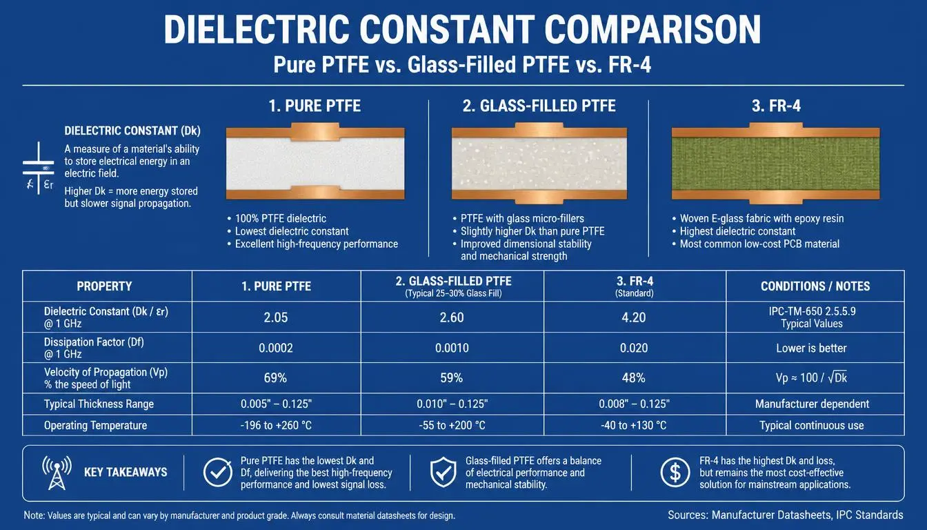
Dielectric Constant Comparison: Pure PTFE vs. Glass-Filled PTFE vs. FR-4
Pure polytetrafluoroethylene (PTFE) has an industry-standard relative permittivity of εr ≈ 2.0–2.2 across typical RF frequencies. That is roughly half the dielectric constant of standard FR-4 (εr ≈ 4.2–4.8), which is why PTFE laminates dominate microwave applications where low loss and stable impedance matter.
However, “Teflon PCB” is not one material. Filler and reinforcement systems push εr higher and change other properties:
Material family | Representative grade | Typical εr (10 GHz) | Typical tanδ |
|---|---|---|---|
Pure PTFE | Generic PTFE film/laminate | 2.0–2.1 | 0.0002–0.0005 |
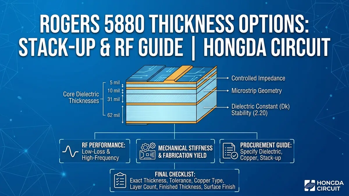
Glass microfiber PTFE | Rogers RT/duroid 5880 | 2.20 | 0.0009 |
Glass microfiber PTFE | Rogers RT/duroid 5870 | 2.33 | 0.0012 |
Ceramic-filled PTFE | Rogers RO3003 | 3.00 | 0.0010 |
Woven glass + PTFE | Taconic TLY-5 | 2.20 | 0.0009 |
Ceramic/glass PTFE | Taconic RF-35 | 3.50 | 0.0018 |
Note how a single “PTFE-based” description covers εr from 2.0 to 3.5. Always confirm the value on the manufacturer’s datasheet for your exact grade, thickness, and resin content — the design equations below are only as good as the number you put into them.
Frequency and Temperature Dependence: εr and Loss Tangent from MHz to Tens of GHz
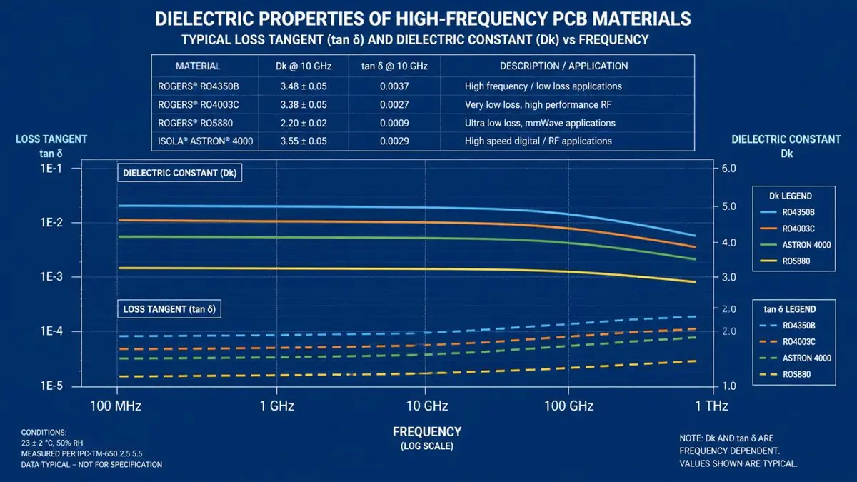
Graph illustrating how dielectric constant ($\varepsilon_r$) and loss tangent ($\tan\delta$) vary across different frequencies and temperature changes for high-frequency PCB materials.
Two numbers on a datasheet — εr and dissipation factor (tanδ) — are rarely constant, and designing as if they are is a common cause of mismatched prototypes.
Frequency behavior. εr for PTFE-based laminates typically drifts only slightly from low MHz into the 1–10 GHz range (on the order of ±1–2%), but tanδ rises with frequency in most practical laminates. As a working reference for glass-filled PTFE (e.g., RT/duroid 5880 class material): tanδ ≈ 0.0005–0.001 below 1 GHz, ≈ 0.0009 at 10 GHz, and ≈ 0.0015–0.002 approaching 40 GHz. Pure PTFE stays lower (≈ 0.0002–0.0005) but offers poor dimensional stability. If your design spans more than one decade of frequency, request εr/tanδ versus frequency curves from the material vendor rather than a single-point value.
Temperature and environment. The dielectric constant of PTFE decreases slightly with temperature (a negative temperature coefficient of permittivity, roughly −100 to −300 ppm/°C depending on filler). More importantly for high-power or automotive/space designs, coefficient of thermal expansion (CTE), glass transition behavior, and moisture uptake change both εr and loss: PTFE absorbs very little moisture (<0.05%), but glass and ceramic fillers raise it, and absorbed moisture raises effective εr and tanδ measurably. For designs operating above 85 °C ambient or with high RF power density, evaluate εr and tanδ at your worst-case temperature — most competitor articles never show temperature curves; the vendor’s characterization report should.
Measuring and Specifying εr and Loss Tangent: Standards and Test Methods
Datasheet values are measured, not theoretical — and if you need to verify a laminate lot or a competitor’s claim, these are the methods that matter:
- Stripline resonator / split-post dielectric resonator (SPDR): the standard reference methods for tanδ and εr at GHz frequencies, referenced by IPC-TM-650 (methods 2.5.5.x series). Use these when you need traceable, frequency-specific numbers.
- Microstrip ring or patch resonator: practical for characterizing finished board stacks; extract εeff from resonant frequency and back out εr.
- Time-domain reflectometry (TDR): fast and non-destructive for εeff along a transmission line; ideal for impedance verification on production panels, less precise for absolute εr.
- Parallel-plate / guarded electrode capacitance methods: suitable below ~1 GHz per IPC-TM-650 2.5.9.
Real-world measurement pitfalls: dielectric thickness variation across the panel (PTFE laminates are softer than FR-4 and compress differently under lamination pressure), copper roughness at the conductor–dielectric interface (raises effective loss at GHz), voids or resin starvation in multilayer bonding, and test-fixture calibration errors. Specify test method, frequency, and temperature whenever you write εr or tanδ into a purchase specification — and prepare coupons from the same lot as production boards for verification.
Design Implications: Effective Permittivity, Impedance Control, and Simulation Models
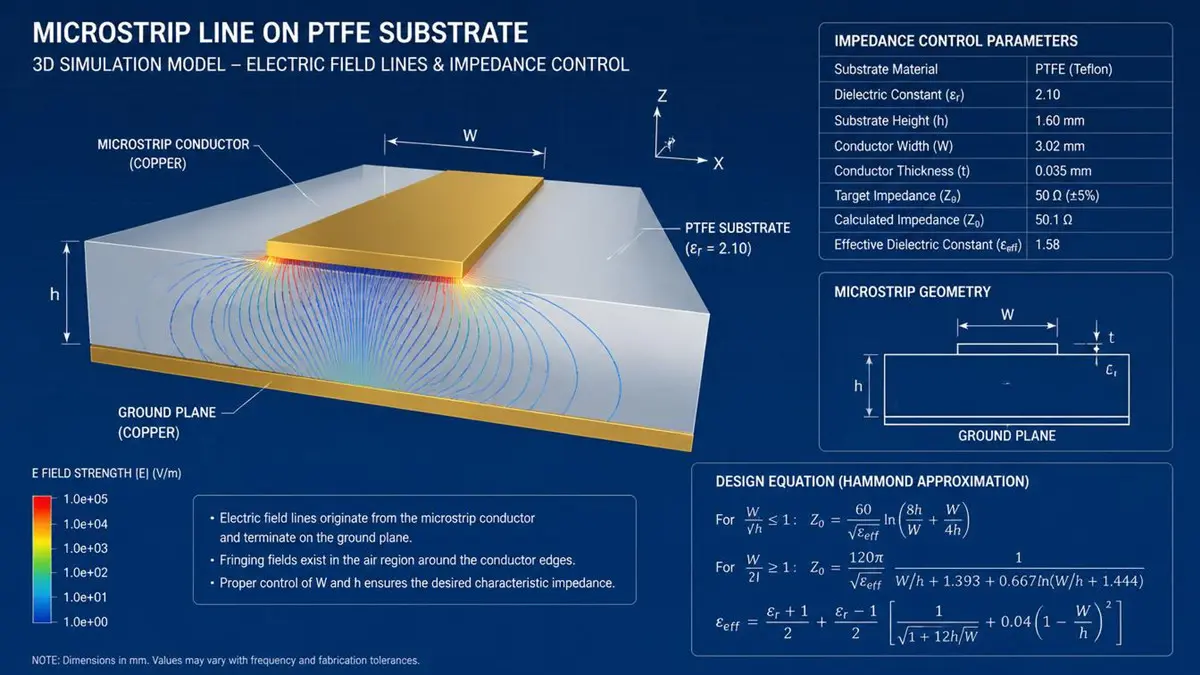
3D Simulation Model of a Microstrip Line on a PTFE Substrate
For a microstrip line, the fields exist partly in the PTFE and partly in air, so you design with the effective permittivity εeff, not bulk εr. For a PTFE substrate with εr = 2.2, εeff typically lands between 1.7 and 1.9 depending on geometry.
Worked example — 50 Ω microstrip on RT/duroid 5880 (εr = 2.2):
- Substrate height h = 0.787 mm (31 mil), 1 oz copper (t ≈ 35 µm)
- Using standard closed-form relations (Hammerstad/Jensen), W ≈ 2.2 mm and εeff ≈ 1.86
- Stripline (embedded between two PTFE layers) uses εr directly: for h = 0.5 mm dielectric to each reference plane, a 50 Ω line is roughly W ≈ 1.1 mm with εeff = εr = 2.2
Then correct for reality: solder mask adds ~0.3–0.5 to effective εr at the surface and lowers impedance by several ohms on outer layers; surface finish (ENIG adds plated nickel) slightly reduces effective conductor thickness; plated through-holes and via fences perturb nearby impedance; and copper roughness increases insertion loss at 10 GHz and above. In HFSS, ADS, or Siemens EDA (HyperLynx/Simcenter), import the full stackup with vendor εr/tanδ at your operating frequency, model solder mask as a separate layer, and validate against a TDR coupon before releasing fabrication — this parameter-pack-plus-coupon workflow is what separates boards that simulate from boards that measure correctly.
Manufacturing, Material Selection, and Sourcing for Teflon PCBs
Material choice drives manufacturability as much as electrical performance:
- Pure PTFE machines and drills poorly, creeps under mechanical load, and cannot be bonded without surface treatment. Use it only where its ultra-low loss (tanδ ≈ 0.0002) genuinely matters.
- Filled PTFE (ceramic, glass microfiber, woven glass) dramatically improves dimensional stability, CTE match to copper, and drilling quality — this is why RF-35, RO3003, and RT/duroid 5880 dominate production designs.
- Bonding and surface activation: PTFE is chemically inert. Multilayer PTFE boards require sodium-naphthalene etching, plasma treatment, or adhesive-coated bonding films (e.g., FEP or thermoset bonding layers), each with different loss and temperature consequences.
- Via plating: smear removal is difficult because PTFE re-flows under drill heat; specialized desmear (plasma) cycles are mandatory, and plated via reliability must be qualified per design.
Cost and lead time reality: PTFE laminates run roughly 5–20× the cost of FR-4 per panel depending on grade, and exotic grades often carry minimum order quantities (MOQs) of 5–10 sheets and 4–12 week lead times. Build your material selection around total cost — impedance-controlled PTFE often eliminates tuning cycles that cost far more than the laminate premium. When comparing suppliers, request the full datasheet package (εr/tanδ vs. frequency and temperature, CTE, peel strength, moisture absorption) rather than a single-page marketing summary.
Get These Values Applied to Your Stackup — Free
Reading parameters is one thing; applying them to a manufacturable stackup is another. We offer three no-obligation next steps:
- Free PTFE laminate quick-reference table — εr, tanδ, CTE, and thickness availability across common Rogers and Taconic grades at your target frequency. Delivered within 24 hours.
- 50 Ω impedance calibration review — upload your stackup file and receive a one-time microstrip/stripline calculation and simulation review, including solder-mask corrections, within 2 business days.
- PTFE PCB fabrication quote (US) — send Gerbers and stackup for a quote with stated lead time, MOQ, and material lot traceability; typical turnaround on quotes is 24 hours.
[Upload your stackup / Request the quick-reference table / Get a fabrication quote →] Email:pcb@pcbcoming.com
FAQ
What is the typical dielectric constant (εr) range for Teflon (PTFE) used in RF PCBs?
Pure PTFE is εr ≈ 2.0–2.2. Filled or reinforced PTFE laminates range from about 2.2 (glass microfiber, e.g., RT/duroid 5880) to 3.0–3.5 (ceramic-filled, e.g., RO3003 or RF-35). Always use the datasheet value for your exact grade and thickness.
How do the dielectric constant and loss tangent of PTFE change between MHz and tens of GHz?
εr is very stable (±1–2% typically). tanδ rises with frequency: roughly 0.0005–0.001 below 1 GHz, ~0.0009 at 10 GHz for glass-filled PTFE, and ~0.0015–0.002 near 40 GHz. Temperature increases slightly reduce εr; moisture absorption increases both εr and tanδ.
Which test methods and standards should I use to measure εr and dissipation factor for PTFE laminates?
Use IPC-TM-650 methods: stripline or split-post dielectric resonator techniques for GHz-range εr/tanδ (2.5.5.x series), parallel-plate capacitance below 1 GHz, and TDR for effective permittivity and impedance verification on production panels. Always state frequency, temperature, and test method.
How do I calculate effective permittivity and design a 50 Ω microstrip on a PTFE substrate?
For εr = 2.2, h = 0.787 mm, 1 oz copper, a 50 Ω microstrip is approximately W ≈ 2.2 mm with εeff ≈ 1.86. For stripline the fields are fully in the dielectric, so εeff = εr. Use field-solver or closed-form equations, then correct for solder mask, copper roughness, and finish effects, and validate with a TDR coupon.
What manufacturing challenges do PTFE PCBs present (via plating, bonding, surface treatment) and how are they mitigated?
Key challenges: PTFE drill smear requiring plasma desmear, chemical inertness requiring sodium etching or plasma activation before bonding, and poor dimensional stability in pure PTFE. Mitigations include filled PTFE grades, adhesive bonding films (FEP/thermoset), plasma processing, and lot-specific impedance coupons.
How do PTFE-based materials compare to FR-4 and other RF laminates (e.g., Rogers or Taconic) in performance and cost for microwave designs?
FR-4 (εr ≈ 4.4, tanδ ≈ 0.02) is cheap but lossy and unstable in εr. PTFE laminates offer εr 2.0–3.5 with tanδ 0.0002–0.002 — roughly 10–100× lower loss — at 5–20× the laminate cost. For any design above ~3 GHz or with tight impedance tolerance, PTFE or PTFE-ceramic hybrids (Rogers, Taconic) typically reduce tuning cycles enough to justify the premium.
About Author
David Chen(K) LinkedIn Profile
David Chen is a Senior RF/PCB Process Engineer at HAODA ELECTRONIC CO.,LIMITED., with over 12 years of experience in high-frequency PCB fabrication, impedance-controlled stack-up design, and Rogers/PTFE laminate processing. He also boasts an extensive professional background in PCBA manufacturing, PCBA testing, and PCBA optimization, with specialized expertise in high-precision PCBA fault analysis and rigorous PCBA reliability testing. The author has worked with high-layer-count server PCB fabrication, ultra-low-loss backplane stackups, and thermo-mechanical reliability optimization for AI infrastructure projects involving 112G and 224G PAM4 architectures. Skilled in complex circuit design and cutting-edge advanced PCB manufacturing processes, he delivers solutions that elevate product durability and performance across industrial applications. His technical articles focusing on PCBA manufacturing workflows and testing methodologies are widely cited by industry peers and technical platforms, and have gained attention and recognition from industry colleagues.