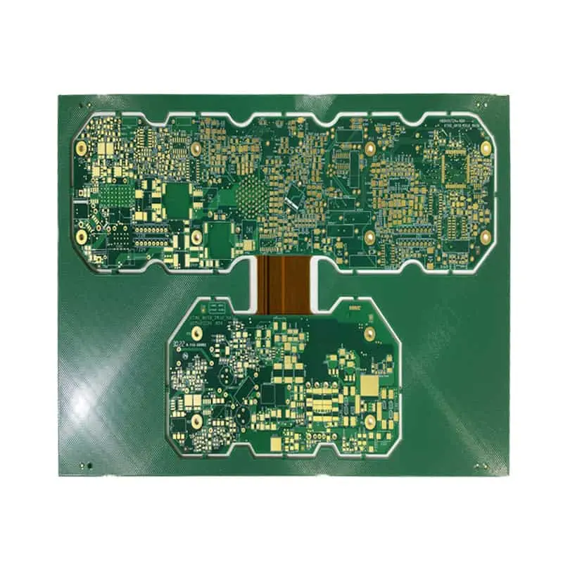
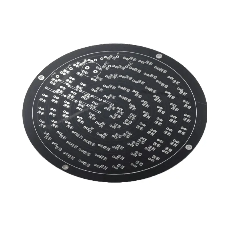
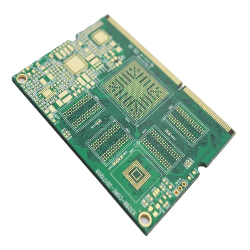
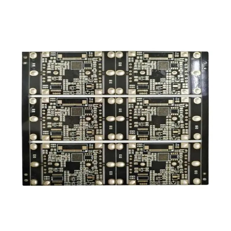
A thermal clad PCB is a circuit board designed to transfer heat away from power-generating components through a thermally conductive dielectric and a metal base or heat-spreading structure. It is commonly considered for LED lighting, power conversion, automotive electronics, and high-power communication equipment where conventional FR-4 may not provide sufficient thermal performance.
Choosing the right thermal clad PCB requires more than specifying thermal conductivity. Engineers and procurement teams must evaluate through-plane thermal resistance, copper thickness, dielectric insulation, bonding reliability, assembly compatibility, and total manufacturing cost. HAODA ELECTRONIC CO.,LIMITED. supports PCB manufacturing and PCBA procurement discussions for customers evaluating application-specific circuit board requirements.
What Is a Thermal Clad PCB and When Should You Use It?
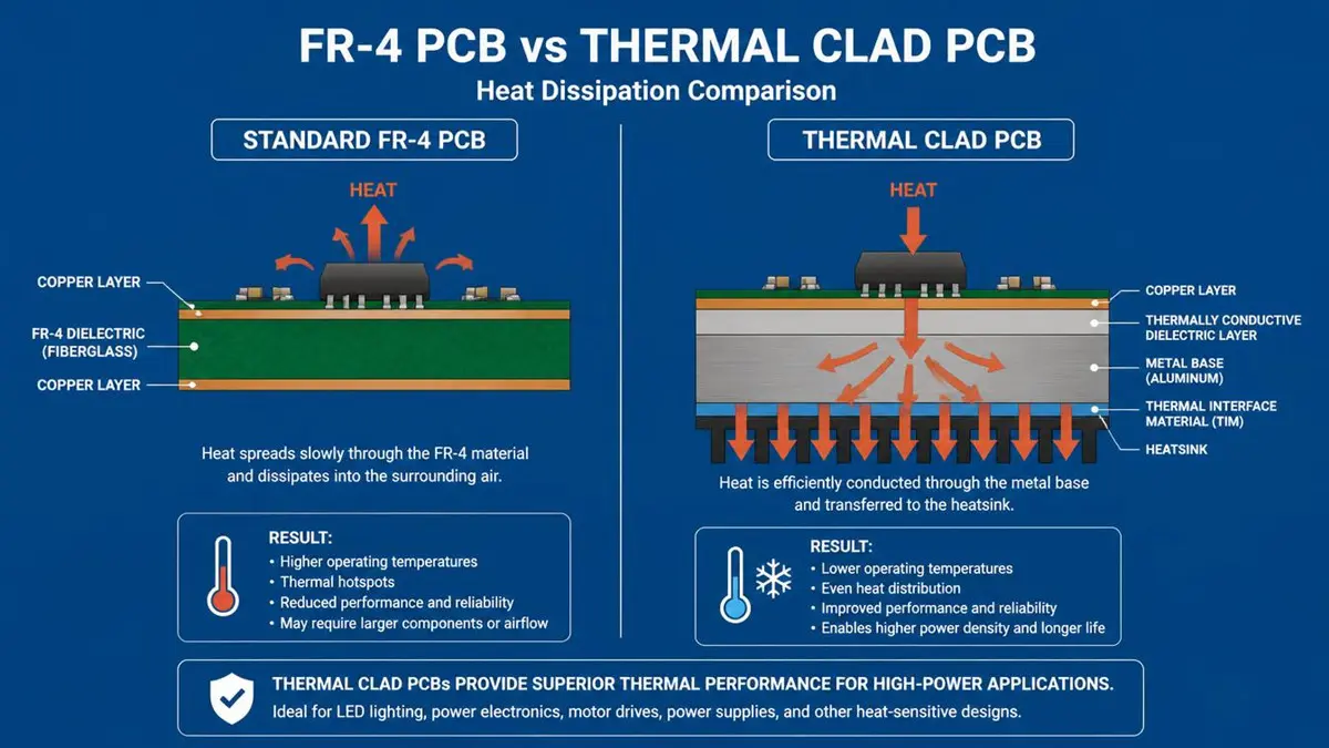
FR-4 PCB vs Thermal Clad PCB Heat Dissipation Comparison
A thermal clad PCB integrates an electrically insulating, thermally conductive layer with a metal structure to improve heat transfer from components to a heat sink or chassis. Depending on the product design, the construction may use an aluminum or copper base, a specialized dielectric bonding layer, or another engineered thermal interface.
Unlike conventional FR-4, which primarily uses glass-reinforced epoxy laminate, a metal-based thermal clad structure provides a more direct heat-spreading path. However, thermal performance depends on the entire stackup, not simply the metal base.
| PCB type | Main advantage | Key limitation | Typical application |
|---|---|---|---|
| FR-4 PCB | Cost-effective, versatile, multilayer routing | Heat spreading may be limited | General electronics and control boards |
| Aluminum IMS PCB | Good heat spreading with an insulated metal substrate | Electrical isolation and routing constraints | LED lighting and power modules |
| Copper-core PCB | High thermal conductivity and heat spreading | Higher material cost and greater weight | High-power and specialized thermal designs |
| Thermal clad PCB | Engineered thermal path tailored to the application | Performance depends on dielectric and bonding construction | Power electronics and thermally demanding assemblies |
When should you choose a thermal clad PCB?
Consider a thermal clad design when component junction temperatures approach their allowable limits, the available cooling area is restricted, or the product requires a controlled thermal path between the component and its mounting structure.
For example, LED modules may need to spread heat across a compact board, while power converters may require efficient heat transfer from switching devices. Automotive electronics may introduce additional vibration and thermal-cycling requirements.
The final selection should be based on measured thermal resistance, electrical isolation requirements, mechanical constraints, and expected operating conditions. A metal-core design is not automatically superior to FR-4 with thermal vias and an external heat sink; the complete assembly must be evaluated.
Thermal Clad PCB Materials, Construction and Measured Thermal Performance
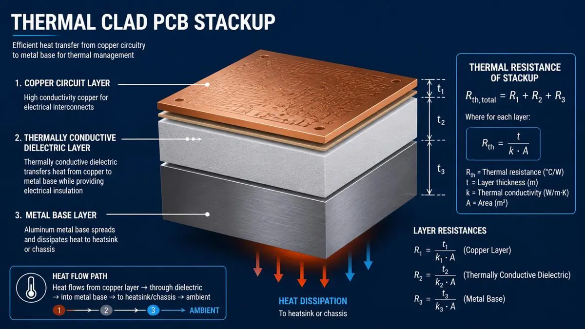
Thermal Clad PCB 3D Stackup and Thermal Resistance Formula
Thermal clad PCB performance depends on the thermal properties and thicknesses of its individual layers.
A typical metal-based structure includes a copper circuit layer, a thermally conductive electrical insulation layer, and a metal base. The copper circuit layer carries current and spreads heat locally. The dielectric provides electrical isolation while conducting heat toward the base. The metal base distributes heat across a larger area and transfers it toward the heat sink or chassis.
Common material options include:
- Aluminum base: Offers a practical balance of thermal spreading, weight, and cost for many LED and power applications.
- Copper base: Provides higher bulk thermal conductivity than aluminum but generally increases material cost and weight.
- Thermally conductive dielectric: Its conductivity, thickness, dielectric strength, and bonding characteristics strongly influence overall thermal resistance.
- Specialized bonding materials: Adhesives or engineered bonding layers must maintain thermal and mechanical integrity during operation.
Direct-bonded copper (DBC) is another construction option, particularly for power electronics and ceramic substrates. It should not be treated as interchangeable with conventional metal-core IMS construction; its material system and manufacturing route are different.
How should thermal performance be measured?
Thermal conductivity, expressed in W/(m·K), describes a material’s ability to conduct heat. Thermal resistance, expressed in K/W or °C/W, describes the temperature difference associated with heat flowing through a defined structure.
For a uniform layer under simplified one-dimensional steady-state conditions:
Rth = t / (k × A)
Where:
- Rth = thermal resistance in K/W
- t = layer thickness in meters
- k = thermal conductivity in W/(m·K)
- A = effective heat-transfer area in square meters
This equation illustrates why a thin, thermally conductive dielectric can be beneficial. Actual board performance also depends on spreading resistance, interfaces, component packages, mounting pressure, and cooling conditions.
Useful validation methods include steady-state thermal-resistance measurements, transient thermal testing, infrared thermography, and controlled power-step experiments. Laser-flash testing can characterize material thermal diffusivity, from which conductivity may be calculated when density and specific heat are known.
For meaningful comparisons, test samples should use the same geometry, heat source, power input, boundary conditions, and measurement locations. Report ambient temperature, mounting method, applied power, and whether the measured resistance represents the dielectric alone or the complete component-to-coolant thermal path.
Do not assume that a copper-core PCB will always outperform an aluminum IMS board in a finished assembly. The result depends on the dielectric, layer geometry, interface quality, and cooling configuration. Request measured data for the proposed construction rather than relying solely on a material datasheet.
Thermal Clad PCB Design Best Practices and Assembly Compatibility
A thermal clad PCB should be designed around both the electrical layout and the complete heat-removal path. Manufacturing feasibility must be considered before the design is released.
Optimize the thermal path
Place high-power components as close as practical to the intended heat-spreading region. Minimize unnecessary thermal-interface layers between the component and the metal base, and verify that the mounting surface makes adequate contact with the heat sink.
For multilayer FR-4 or hybrid constructions, thermal vias can transfer heat from component-side copper to internal or opposite-side copper planes. Initial design studies may evaluate via diameters around 0.20–0.30 mm and pitches around 0.8–1.2 mm, where appropriate for the fabrication process. These are starting points for engineering evaluation, not universal manufacturing rules.
Thermal via effectiveness depends on barrel plating, via filling, copper thickness, pad geometry, and the available heat-spreading area. For metal-core boards, confirm whether the proposed construction actually supports the required via architecture.
Specify copper thickness and electrical performance
Higher copper weight can reduce electrical resistance and improve local heat spreading, but it also affects etching, minimum spacing, feature definition, and manufacturing cost.
The appropriate copper thickness should be selected using current-carrying requirements, temperature-rise calculations, voltage drop, and fabrication constraints. Confirm trace width, spacing, pad geometry, and finished copper thickness with the manufacturer.
Check surface finish and assembly compatibility
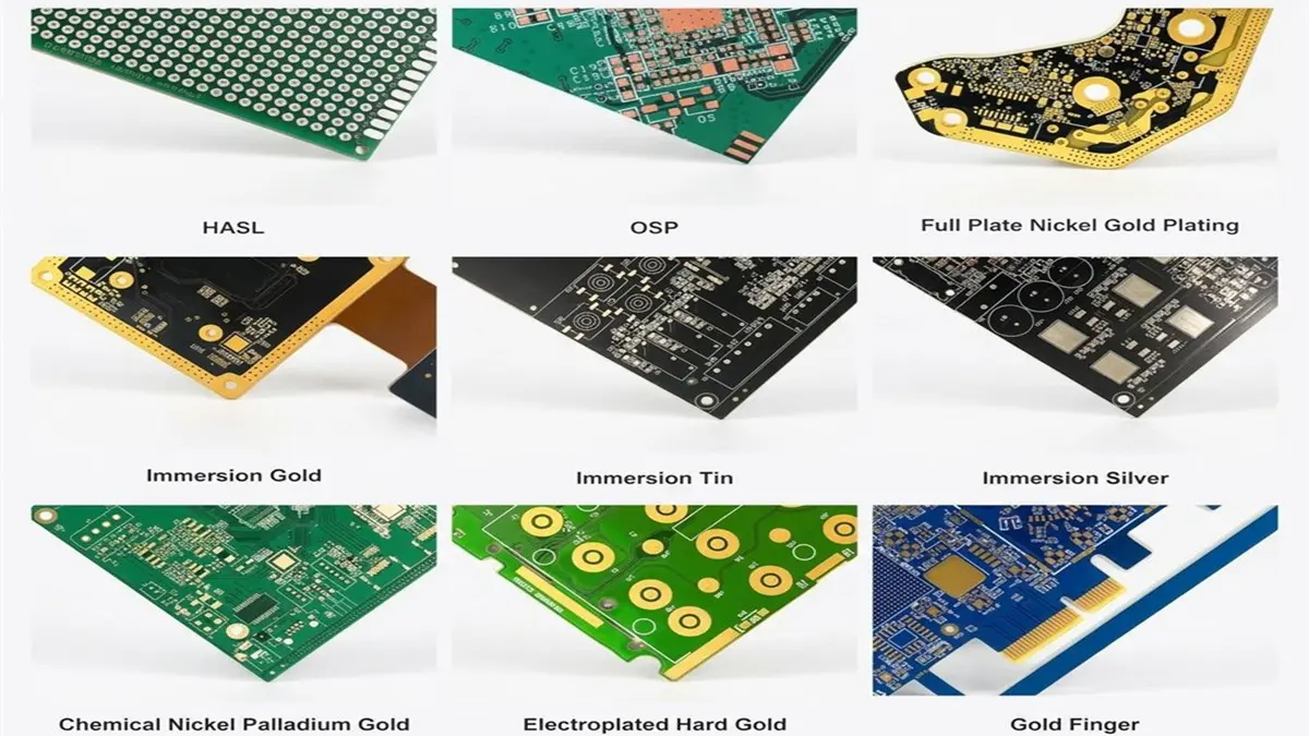
ENIG, HASL, and OSP are common PCB surface-finish options, but suitability depends on component termination, assembly requirements, shelf life, and the selected manufacturing process.
Before production, confirm:
- The solderability of the selected finish and copper structure.
- The permissible reflow temperature profile for the complete board construction.
- Whether the dielectric and bonding materials tolerate repeated thermal exposure.
- The compatibility of the board with solder paste, flux, and cleaning chemistry.
- Whether component replacement can be performed without damaging the dielectric or bond interface.
During rework, use controlled localized heating and the component supplier’s recommended temperature limits. Avoid excessive dwell time, mechanical force, and repeated heating cycles. Inspect the repaired area for lifted pads, delamination, solder defects, and damage to nearby components.
Finally, evaluate thermal expansion mismatch between copper, aluminum, dielectric, ceramic, and mounted components. Appropriate material selection, compliant interfaces, mechanical support, and controlled fastening can help reduce stress during thermal cycling.
Thermal Clad PCB Manufacturing, Bonding Processes, Tolerances and Qualification
Thermal clad PCB manufacturing may involve adhesive lamination, thermally conductive dielectric bonding, or specialized direct-bonding processes, depending on the selected material system.
In adhesive-based construction, lamination temperature, pressure, time, and surface preparation influence bond integrity, dielectric thickness, void formation, and dimensional stability. Excessive process variation can increase thermal resistance or cause delamination.
Direct-bonded copper and ceramic-based constructions follow different manufacturing routes and require process-specific controls. A supplier should identify the actual construction rather than using terms such as thermal clad, IMS, and DBC interchangeably.
Which tolerances should procurement specify?
The drawing and purchase specification should define, as applicable:
- Finished board thickness and dielectric thickness.
- Copper thickness and acceptable feature geometry.
- Board flatness and dimensional tolerances.
- Base-metal thickness and surface condition.
- Bond integrity and applicable peel or adhesion requirements.
- Electrical insulation and dielectric-withstand requirements.
- Thermal performance acceptance criteria.
Do not accept a quoted tolerance without confirming that it applies to the selected material stackup and production process. Similarly, a generic yield percentage is not a reliable basis for procurement unless it is supported by relevant production data.
How should thermal clad PCBs be qualified?
A practical qualification plan should include visual inspection, dimensional verification, electrical testing, thermal-performance measurement, and bond-integrity evaluation.
For demanding applications, consider thermal cycling, high-temperature exposure, humidity testing, and mechanical testing as appropriate to the product environment. IPC, UL, and JEDEC documents may be relevant, but each applies within a particular scope; the correct standard and acceptance criteria must be agreed upon for the specific board and end product.
For prototypes, allow time for material confirmation, stackup review, fabrication, assembly if required, and thermal validation. Lead time should be confirmed against actual material availability and process complexity rather than assumed from a generic industry estimate.
If a board fails qualification, investigate the failure mechanism before attempting repair. Localized heating or machining may be feasible for some defects, but delamination or damage to an insulated metal interface can make the assembly unsuitable for repair. Rework should follow an approved procedure and be followed by appropriate retesting.
Thermal Clad PCB Applications, Cost and Supplier Selection
Thermal clad PCBs are used in applications where heat generation, available cooling space, and reliability requirements make thermal management a critical design consideration.
Common applications include:
- LED lighting: High-power LED modules, industrial lighting, and compact luminaires.
- Power conversion: Switching power supplies, DC-DC converters, and power-control assemblies.
- Automotive electronics: Selected power modules and electronic assemblies exposed to demanding thermal environments.
- Telecommunications: Power distribution and selected RF or communication equipment requiring effective heat spreading.
There is no single power threshold that determines when a thermal clad PCB becomes necessary. Component package, heat flux, operating temperature, cooling airflow, and allowable junction temperature all influence the decision.
What determines thermal clad PCB cost?
The main cost drivers include base-metal type and thickness, dielectric material, copper weight, board dimensions, layer count, special bonding processes, surface finish, testing requirements, and order quantity.
Prototype pricing should be evaluated separately from volume production because tooling, engineering review, material procurement, and setup costs are distributed across different quantities. A reliable quote requires a defined specification rather than an unsupported universal price range.
When evaluating suppliers, request:
- A material stackup identifying the dielectric, metal base, and bonding process.
- Relevant thermal conductivity data and measured thermal-resistance results.
- Electrical insulation and dielectric-withstand test results where required.
- Bond-integrity, dimensional, and copper-thickness inspection data.
- Reliability test plans and qualification records relevant to the application.
- Traceability, change-control procedures, and applicable quality certifications.
- A clear quotation covering tooling, testing, lead time, and production quantities.
For example, an LED manufacturer experiencing excessive board temperatures should compare candidate constructions using the same LED power, board geometry, mounting interface, and cooling conditions. Infrared images can reveal hot spots, while temperature measurements and a controlled power input help quantify the improvement. This is a recommended validation approach, not a claim of a completed customer project.
Reduce procurement risk by approving a representative prototype, agreeing on measurable acceptance criteria, and qualifying the design before volume production. Include material substitutions, change notification, inspection documentation, and failure-handling requirements in the purchase agreement.
Request a Thermal Clad PCB Quote from HAODA ELECTRONIC CO.,LIMITED
Selecting a thermal clad PCB supplier is easier when the thermal target, electrical requirements, and production scope are clearly defined. HAODA ELECTRONIC CO.,LIMITED works with customers evaluating PCB manufacturing and assembly requirements for electronic products.
To request a technical review or quotation, provide:
- Board dimensions and finished thickness.
- Required copper thickness and number of layers.
- Preferred base metal and dielectric, if already specified.
- Component power dissipation and maximum allowable temperature.
- Target thermal resistance or other thermal acceptance criteria.
- Required surface finish and electrical insulation specifications.
- Prototype quantity, expected annual volume, and required delivery date.
Send your requirements to pcb@pcbcoming.com or to discuss your project.
Where available and agreed for the project, request supporting thermal measurements, infrared thermography, and reliability test documentation. If your design is still at the engineering stage, begin with a stackup review and define the validation plan before committing to production.
The objective is not simply to purchase a thermally conductive board. It is to select a manufacturable construction that meets the product’s thermal, electrical, mechanical, and commercial requirements.
Frequently Asked Questions About Thermal Clad PCBs
What is a thermal clad PCB, and when should I choose it over FR-4, aluminum IMS, or copper-core PCBs?
A thermal clad PCB uses an engineered thermal path, often incorporating a conductive dielectric and metal base. Consider it when conventional FR-4 cannot meet the thermal target within the available space. Compare aluminum IMS, copper-core, and alternative constructions using the same operating conditions and complete-assembly thermal resistance.
How is thermal performance measured, and what thermal resistance should I expect?
Thermal performance can be evaluated using steady-state resistance measurements, transient testing, infrared thermography, and material characterization. Expected values depend on layer thickness, conductivity, heat-transfer area, interfaces, and test conditions. Specify a measurable acceptance target and request supporting test data for the actual stackup.
Which PCB layout and DFM rules improve heat dissipation?
Prioritize a short, continuous thermal path, sufficient copper area, appropriate component placement, and effective heat-sink contact. Thermal vias can help in suitable multilayer constructions. Confirm via geometry, copper thickness, spacing, and manufacturing limits with the supplier before finalizing the layout.
Which bonding processes affect manufacturing lead time, tolerances, and yield?
Adhesive lamination, engineered dielectric bonding, and direct-bonding technologies have different material, equipment, and process-control requirements. Their effects on lead time and yield depend on the selected construction and manufacturing route. Request process-specific tolerances, inspection criteria, and relevant production evidence.
Are thermal clad PCBs compatible with standard solder finishes and reflow assembly?
Potentially, yes. ENIG, HASL, and OSP may be suitable depending on the board design and assembly process. Confirm solderability, allowable thermal exposure, and compatibility with the dielectric and bonding materials. Validate the reflow profile before production and use controlled heating during rework.
What determines prototype and production pricing in the United States?
Cost depends on materials, dimensions, copper weight, layer count, bonding complexity, surface finish, testing, order quantity, and delivery requirements. Request separate prototype and volume quotations based on the same technical specification. This enables a meaningful comparison of engineering costs, unit prices, and total procurement costs.
Which reliability tests should I request from a thermal clad PCB supplier?
Depending on the end-use environment, request thermal cycling, humidity exposure, high-temperature testing, mechanical evaluation, electrical insulation testing, and bond-integrity assessment. Define the applicable test method, sample quantity, acceptance criteria, and reporting requirements before qualification begins.
About Author
David Chen LinkedIn Profile
David Chen is a Senior RF/PCB Process Engineer at HAODA ELECTRONIC CO.,LIMITED., with over 12 years of experience in high-frequency PCB fabrication, impedance-controlled stack-up design, and Rogers/PTFE laminate processing. He also boasts an extensive professional background in PCBA manufacturing, PCBA testing, and PCBA optimization, with specialized expertise in high-precision PCBA fault analysis and rigorous PCBA reliability testing. The author has worked with high-layer-count server PCB fabrication, ultra-low-loss backplane stackups, and thermo-mechanical reliability optimization for AI infrastructure projects involving 112G and 224G PAM4 architectures. Skilled in complex circuit design and cutting-edge advanced PCB manufacturing processes, he delivers solutions that elevate product durability and performance across industrial applications. His technical articles focusing on PCBA manufacturing workflows and testing methodologies are widely cited by industry peers and technical platforms, and have gained attention and recognition from industry colleagues.