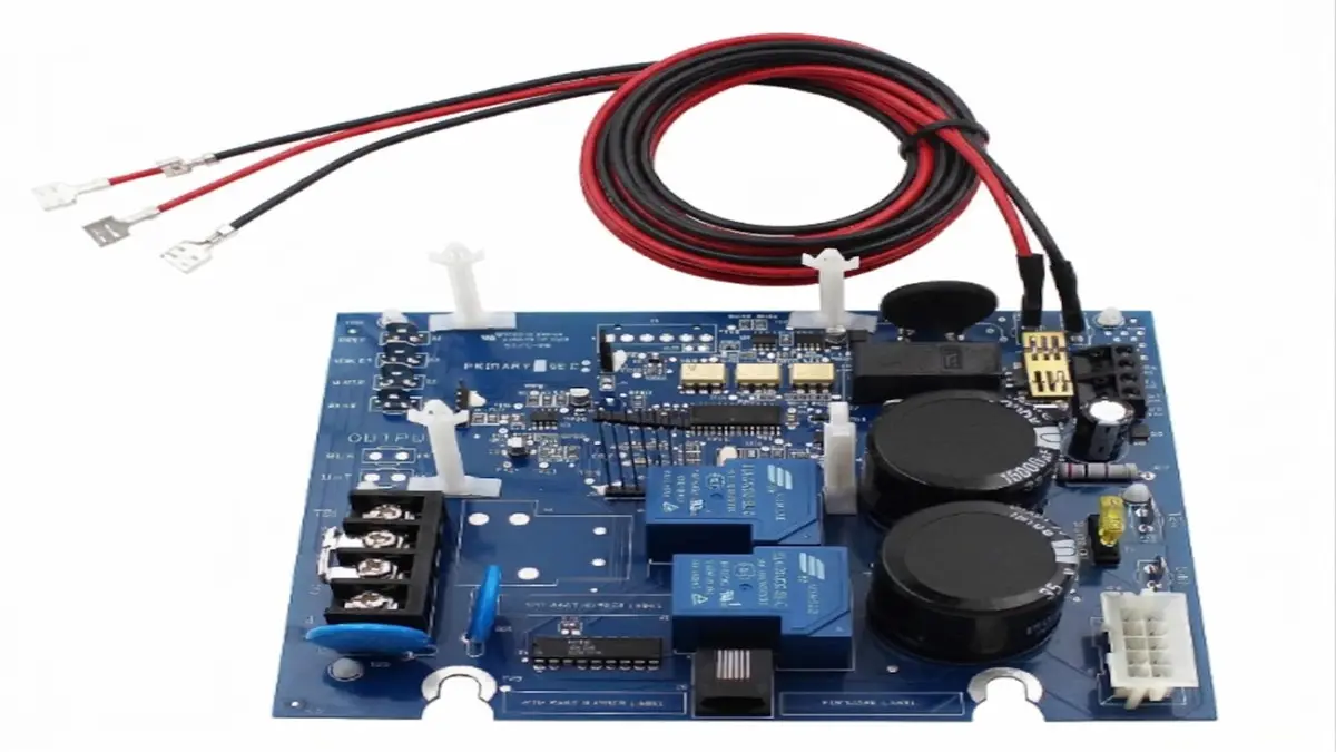
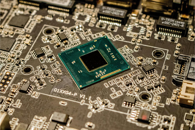
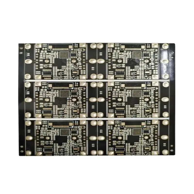
Broken Circuit in PCB can stem from cracked solder joints, fractured copper traces, damaged vias, corrosion, thermal stress, or manufacturing defects. Since the proper remediation hinges on the exact location of the interrupted electrical path, the root cause of failure, and whether the impairment undermines long-term reliability, engineers must complete fault diagnosis prior to carrying out any repair work. If the board’s reliability cannot be validated after remediation, component or board replacement should be considered instead.
For electronics manufacturers, the most robust strategy integrates structured failure analysis, well-informed repair judgements, design-for-manufacturability (DFM) rules, and consistent, high-quality PCB fabrication. Mastery of these contributing factors minimizes production downtime, prevents recurring field failures, and elevates overall product quality.
1. What Causes Broken Circuits in PCBs, and How Can You Identify the Failure?
A broken circuit in a PCB occurs when an electrical connection becomes interrupted or develops excessive resistance. Although the symptoms may look similar, the underlying causes can differ significantly between manufacturing defects and damage that occurs during operation.
| Failure symptom | Possible root cause | Common occurrence |
|---|---|---|
| Intermittent electrical connection after heating and cooling | Cracked solder joint or copper fatigue | Industrial controllers, automotive electronics |
| Open circuit inside a multilayer board | Damaged via, plated-barrel crack, or internal trace fracture | High-layer-count boards exposed to thermal stress |
| Green, black, or discolored copper areas | Corrosion, chemical contamination, or oxidation | Humid environments and boards exposed to contaminants |
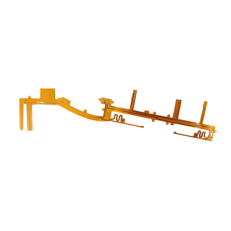
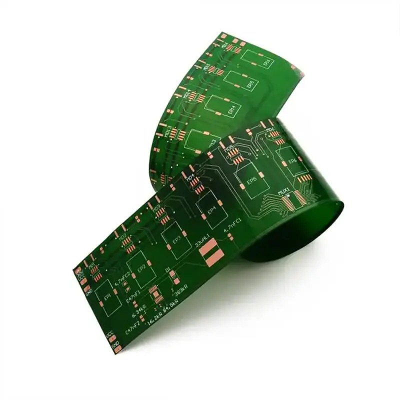
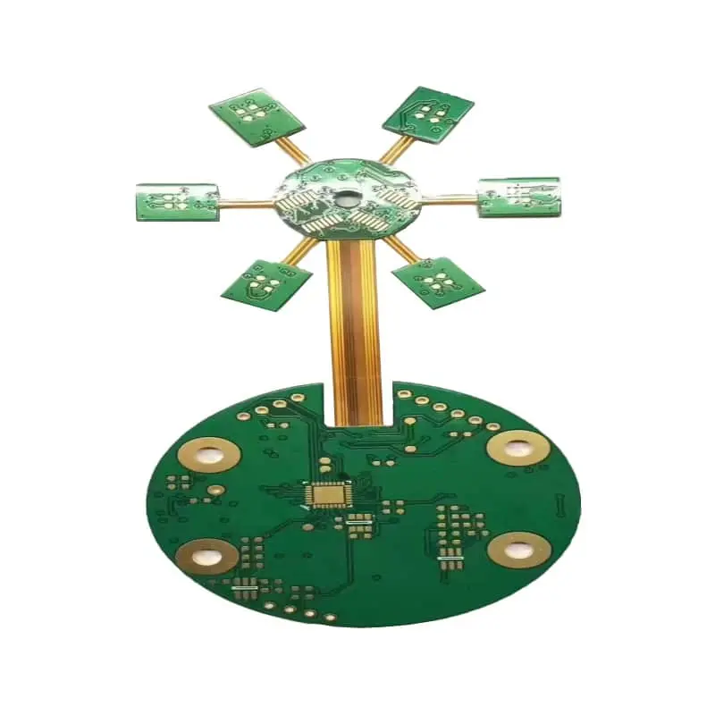
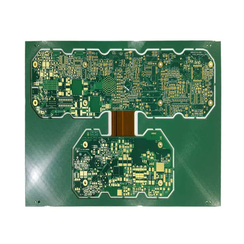
| Cracks near flexible sections | Excessive bending, poor bend-radius design, or copper fatigue | Flexible circuits and rigid-flex assemblies |
| A circuit stops working despite intact visible traces | Failed component, damaged pad, or hidden interconnection defect | Consumer electronics and embedded systems |
| Open circuits detected during production testing | Etching defects, incomplete copper plating, or other fabrication-related discontinuities | Newly manufactured bare PCBs |
Thermal stress deserves particular attention. Repeated temperature changes cause materials with different coefficients of thermal expansion to expand and contract at different rates. Over time, this can fatigue solder joints or damage via structures, especially when the board design, materials, or fabrication quality are unsuitable for the application.
However, a failed board is not automatically evidence of a manufacturing defect. A board that passes initial electrical testing may subsequently fail because of vibration, mechanical impact, overheating, corrosion, or improper assembly.
The distinction matters for procurement teams. A manufacturing-related discontinuity should trigger a review of fabrication records and electrical test results. A field-use failure may instead require examination of operating temperature, mechanical loading, assembly processes, and product design.
Identifying the failure mechanism before selecting a corrective action helps prevent recurring defects in replacement boards.
2. How Can You Diagnose a Broken PCB Using Visual Inspection and Continuity Testing?
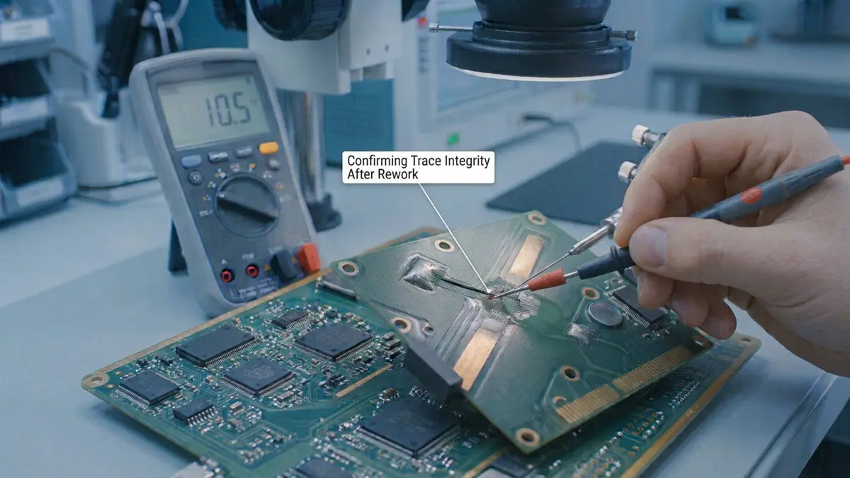
A reliable diagnosis begins with non-destructive inspection and progresses to electrical measurements. The objective is to isolate the failed connection without creating additional damage.
Step 1: Inspect the PCB Before Applying Power
Disconnect the board from its power source and discharge stored energy according to the equipment’s safety requirements.
Inspect the board under adequate lighting or magnification. Look for:
- Cracked solder joints around connectors, heavy components, and mechanically stressed areas.
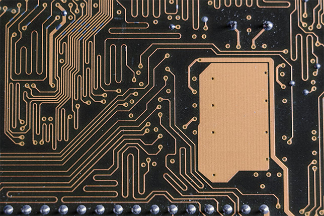
- Scratched or fractured copper traces.
- Burn marks, blistering, delamination, and unusual discoloration.
- Corrosion, conductive contamination, and damaged solder mask.
- Cracked vias, lifted pads, and damaged component leads.
A visual inspection can identify obvious faults, but it cannot reliably exclude internal cracks or defects beneath components.
Step 2: Check Continuity Across the Suspected Circuit
Use a digital multimeter in continuity or resistance mode, with the board unpowered.
Identify the suspected net from the schematic, PCB layout, or test documentation. Select accessible test points on both sides of the suspected break and measure the connection.
For a known continuous copper path, a stable, low resistance consistent with the path’s expected resistance supports electrical continuity. An open-circuit reading may indicate a broken trace, failed via, disconnected component, or incorrect test-point selection.
There is no universal resistance threshold for every PCB connection. The acceptable value depends on trace geometry, copper thickness, connection length, component paths, and measurement setup. A continuity buzzer alone is insufficient when the circuit requires precise resistance measurements.
For example, if a connector pin and its corresponding downstream test point should share the same copper net, an unexpected open reading suggests a discontinuity between them. Check the schematic and intermediate connections before concluding that the trace itself is broken.
Step 3: Isolate the Fault
If the suspected path includes parallel branches, resistors, semiconductor devices, or other components, in-circuit measurements may produce misleading results.
Compare measurements with the schematic and, where available, a known-good board. Use a four-wire Kelvin measurement when low resistance must be measured accurately. Flying-probe testing can help locate opens and shorts on accessible bare-board test structures, while X-ray inspection and cross-section analysis may be appropriate for suspected internal defects.
Step 4: Decide Whether Further Analysis Is Necessary
Use this practical decision tree:
- Visible trace damage and a confirmed open circuit? Evaluate whether a localized repair is technically appropriate.
- No visible damage, but continuity is abnormal? Check alternative current paths, connectors, vias, and component connections.
- The fault appears only when the board heats, cools, or vibrates? Investigate intermittent connections and mechanical or thermal stress.
- The fault is internal, widespread, or associated with delamination? Consider specialist failure analysis or board replacement.
For production procurement, retain the test results, board revision, lot information, and relevant failure conditions. These records help suppliers investigate recurring problems and determine whether a fabrication-process change is necessary.
3. Can a Broken PCB Be Repaired, or Is Replacement the Better Choice?
A broken PCB can sometimes be repaired, but the decision depends on the damage location, circuit function, board construction, and required service life.
Localized trace damage may be repairable when the affected conductor is accessible and the repair can restore the required electrical and mechanical performance. A qualified technician may remove damaged solder mask, prepare the copper, install an appropriate conductor or jumper, and secure the repair using a suitable insulating or protective material.
Damaged solder joints may be reworked when the pads, component leads, and underlying laminate remain sound. The technician must select a suitable soldering profile and minimize repeated heating, which can lift pads or damage the laminate.
Damaged vias and plated through-holes require greater caution. A via may connect several internal layers, so an external jumper does not automatically restore every intended connection. Repair methods must account for the original net structure, insulation requirements, and electrical performance.
Before authorizing a repair, consider these factors:
| Decision factor | Repair may be appropriate when | Replacement is generally preferable when |
|---|---|---|
| Damage extent | The fault is localized and accessible | Damage is widespread or affects multiple internal layers |
| Board value | The board is expensive, obsolete, or difficult to replace | A replacement board is readily available |
| Reliability requirements | The repair can be inspected and validated | Long-term performance cannot be demonstrated |
| Production schedule | Repair avoids a significant and acceptable delay | Repeated rework creates greater schedule risk |
| Documentation | The repair can be documented and approved | Product requirements prohibit the proposed modification |
For industrial, automotive, medical, and other safety-critical applications, repair decisions must follow the applicable product requirements and approval procedures.
A repaired prototype may be useful for debugging, but it should not automatically be treated as equivalent to a newly manufactured board for production release.
For OEMs and hardware developers, the total cost of ownership matters more than the immediate repair price. Compare technician labor, downtime, retesting, failure risk, and replacement lead time before choosing a solution.
4. How Can PCB Design and Manufacturing Prevent Broken Traces and Circuit Failures?
Preventing broken circuits starts before fabrication. Good PCB design reduces mechanical stress, supports reliable manufacturing, and makes faults easier to detect.
Apply DFM Rules Before Releasing Gerber Files
Review copper spacing, trace width, annular rings, drill sizes, solder-mask clearances, and copper-to-edge distances against the selected manufacturer’s capabilities.
Do not assume that a design rule suitable for one fabrication process will work equally well with another. Fine-line features, small vias, and complex multilayer structures require process-specific controls.
For example, high-density interconnect designs with microvias need careful consideration of via geometry, plating quality, layer transitions, and the intended interconnection structure. A nominally manufacturable design may still present reliability risks if its stackup and process assumptions are not aligned.
Reduce Mechanical and Thermal Stress
Avoid routing sensitive traces through areas exposed to repeated bending, mounting stress, or excessive connector loading. For flexible PCBs, establish an appropriate bend radius and follow the material and copper-construction requirements for the intended flexing conditions.
For multilayer boards, review the stackup, material selection, copper distribution, and thermal environment. Applications exposed to frequent temperature changes may require more detailed thermal-reliability evaluation.
Protect Signal Integrity and Electrical Performance
Impedance-controlled traces, return paths, grounding, and appropriate routing geometry help maintain signal integrity in high-speed circuits. Although signal-integrity problems do not necessarily indicate a broken copper trace, they can produce symptoms that resemble circuit failure.
Similarly, excessive voltage drop or unstable power delivery may be mistaken for an open connection. Diagnose the actual electrical behavior before modifying the PCB layout.
Use a Preproduction Reliability Checklist
Before releasing a design for manufacturing, confirm that:
- The stackup and materials match the application’s electrical, thermal, and mechanical requirements.
- Critical nets have appropriate trace widths and copper thickness.
- Via structures and drilling specifications are compatible with the selected process.
- Flexible regions have suitable bend geometry and copper construction.
- Manufacturing tolerances and inspection criteria are documented.
- Electrical testing covers the required open- and short-circuit checks.
- Environmental testing is defined according to the product’s actual operating conditions.
A qualified manufacturing partner can review these details before production, helping identify preventable defects before they become expensive field failures.
5. How Should You Validate a PCB After Repair or Manufacturing?
A PCB that works immediately after repair has not necessarily demonstrated long-term reliability. Validation should confirm electrical continuity, functional performance, and suitability for the intended operating environment.
Start with a visual inspection of the repaired area or newly manufactured board. Check for lifted pads, solder bridges, contamination, damaged solder mask, and other workmanship concerns.
Next, repeat continuity and resistance measurements on the affected nets. Compare the results with the schematic, design requirements, and baseline measurements where available.
Then perform functional testing under controlled conditions. Verify relevant power rails, input and output signals, communication interfaces, and other application-specific functions.
Environmental testing should be selected according to the actual failure mechanism and product requirements. Thermal cycling may help investigate temperature-related failures, while vibration testing may be appropriate for products exposed to mechanical stress. These tests should use defined acceptance criteria rather than arbitrary cycle counts.
What Can Real Failure Investigations Teach Engineers?
The following are illustrative engineering scenarios, not documented Haoda customer cases.
Case 1: Intermittent industrial controller. A controller resets after repeated heating and cooling. Visual inspection finds no obvious damage, but continuity changes when the board temperature changes. Investigation identifies a suspected cracked solder joint near a mechanically stressed connector. After an approved repair, the team repeats electrical and functional tests under representative thermal conditions.
Case 2: Multilayer board with an internal open. A board fails continuity testing even though its external traces appear intact. Further analysis identifies a suspected internal interconnection defect. The team reviews fabrication and test records before deciding whether the board can be repaired or must be replaced.
Case 3: Flexible circuit failure. A flex circuit develops intermittent connectivity near a repeatedly bent section. The investigation examines bend geometry, copper construction, and the product’s movement profile. The corrective action addresses the mechanical design rather than simply replacing the damaged conductor.
For every investigation, record the symptom, root cause, corrective action, test results, and approval status. This information supports traceability and helps prevent the same failure from recurring in future production.
6. How Can Haoda Help Reduce PCB Manufacturing and PCBA Reliability Risks?
For OEMs, electronics startups, and engineering teams, preventing broken circuits requires more than troubleshooting individual boards. It requires a manufacturing partner that can evaluate design requirements, fabricate the intended circuit structure, and support appropriate inspection and electrical verification.
Shenzhen Hongda Circuit Technology Co., Ltd. provides PCB fabrication and PCBA manufacturing services for customers developing electronic products. Depending on the project requirements, buyers can discuss prototype production, small batches, mass production, and assembly requirements.
When preparing an RFQ, provide the following information:
- PCB design files: Gerber files or other accepted fabrication data, together with drill files and the layer stackup.
- Technical specifications: Board dimensions, layer count, copper thickness, material requirements, surface finish, and controlled-impedance requirements, if applicable.
- Failure information: Photographs, suspected open-circuit locations, test results, and any known operating conditions.
- Production requirements: Prototype or production quantity, target delivery date, and assembly scope.
- Quality requirements: Electrical test coverage, inspection criteria, traceability needs, and any application-specific reliability requirements.
This information helps the manufacturing team assess the project and identify questions that should be resolved before production.
Request a PCB manufacturing or PCBA quotation: Send your project details to pcb@pcbcoming.com
Whether you are developing a new product, replacing a defective board, or investigating recurring electrical failures, early engineering communication can help reduce avoidable manufacturing risks and support a more reliable production process.
Frequently Asked Questions About Broken Circuits in PCBs
What Are the Most Common Causes of PCB Failure in Real-World Electronics?
Common causes include cracked solder joints, fractured copper traces, damaged vias, corrosion, component failures, overheating, mechanical stress, and manufacturing defects. The most likely cause depends on the failure symptoms and operating environment.
How Can You Tell Whether a PCB Is Actually Broken Before Removing Components?
Begin with visual inspection and unpowered continuity testing. Compare measurements against the schematic and expected circuit behavior. If parallel paths or components affect the readings, further isolation may be necessary before confirming an open circuit.
What Is the Most Reliable Way to Test a Broken Trace for Continuity?
Measure between two accessible test points on the same intended net using a multimeter. Confirm that the measurement is consistent with the expected path resistance. For very low resistance, a four-wire Kelvin measurement may improve accuracy.
Can a Broken PCB Be Repaired, and When Is Replacement Better?
Localized trace or solder-joint damage may be repairable if the board structure remains sound and the repair can be validated. Replacement is generally preferable when damage is extensive, internal connections cannot be restored reliably, or product requirements do not permit the proposed repair.
How Do You Validate a PCB Repair So It Does Not Fail Again?
Perform visual inspection, repeat electrical measurements, run functional tests, and conduct appropriate environmental testing when required. Document the results and obtain the necessary engineering approval before returning the board to service.
Which PCB Failures Are Manufacturing Defects Rather Than Field-Use Damage?
Potential manufacturing defects include incomplete copper plating, etching-related discontinuities, and other fabrication defects that create opens or shorts. However, a failure observed after shipment does not establish its cause. Fabrication records, electrical test results, assembly history, and physical analysis may be needed to distinguish manufacturing defects from field damage.
Can AI Tools Like ChatGPT Help With PCB Design or Troubleshooting?
AI tools can help engineers interpret error messages, organize diagnostic steps, review design concepts, and generate preliminary checklists. However, AI-generated conclusions must be verified against the schematic, PCB design files, component datasheets, manufacturing specifications, and actual test measurements. AI should not replace electrical testing or qualified engineering approval.
Planning a new PCB or PCBA project? Contact Shenzhen Hongda Circuit Technology Co., Ltd. at pcb@pcbcoming.com with your design files, technical specifications, quantity, and reliability requirements to discuss manufacturing feasibility and request a quotation.
About Author
David Chen LinkedIn Profile
David Chen is a Senior RF/PCB Process Engineer at Shenzhen Hongda Circuit Technology Co., Ltd., with over 12 years of experience in high-frequency PCB fabrication, impedance-controlled stack-up design, and Rogers/PTFE laminate processing. He also boasts an extensive professional background in PCBA manufacturing, PCBA testing, and PCBA optimization, with specialized expertise in high-precision PCBA fault analysis and rigorous PCBA reliability testing. The author has worked with high-layer-count server PCB fabrication, ultra-low-loss backplane stackups, and thermo-mechanical reliability optimization for AI infrastructure projects involving 112G and 224G PAM4 architectures. Skilled in complex circuit design and cutting-edge advanced PCB manufacturing processes, he delivers solutions that elevate product durability and performance across industrial applications. His technical articles focusing on PCBA manufacturing workflows and testing methodologies are widely cited by industry peers and technical platforms, and have gained attention and recognition from industry colleagues.