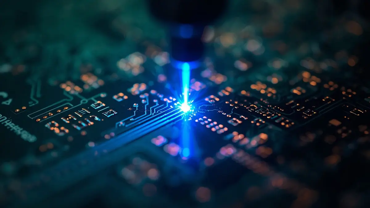
Laser annealing semiconductor processing delivers localized heating of semiconductor substrates, enabling rapid recrystallization and dopant activation while minimizing thermal damage to adjacent device structures. For semiconductor manufacturers, optimal process tuning relies on multiple critical parameters: laser wavelength, laser fluence, pulse duration, melt depth, material compatibility, target electrical performance, and validated production throughput.
Selecting a laser annealing system is far more than just opting for higher laser power. Procurement teams need to evaluate whether the equipment can satisfy stringent electrical specifications, sustain consistent wafer-to-wafer uniformity, preserve thermally vulnerable structures, and achieve a viable cost per processed wafer.
- How Does Melting and Recrystallization Work in Laser Annealing?
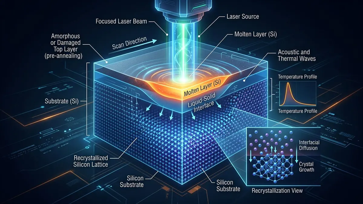
Laser annealing semiconductor melting and recrystallization process diagram on silicon wafer
Laser annealing uses controlled optical energy to heat a semiconductor surface, sometimes above its melting point, allowing the material to recrystallize as it cools. This process can activate implanted dopants, repair implantation damage, and modify defects without heating the entire wafer to the same temperature.
Three physical mechanisms determine the result.
First, the semiconductor absorbs incident laser energy according to its wavelength, optical properties, surface condition, and temperature. The resulting thermal profile establishes whether the treatment remains in the solid phase or creates a molten surface layer.
Second, when melting occurs, the liquid–solid interface advances into the material. As the melt solidifies, the underlying crystalline substrate can guide epitaxial regrowth. Melt depth depends on absorbed energy, pulse duration, heat conduction, and material properties—not pulse energy alone.
Third, rapid solidification redistributes defects and incorporates dopant atoms into substitutional lattice sites. Properly controlled recrystallization can improve electrical activation while limiting the diffusion associated with longer furnace treatments.
For engineering reference, laser pulse durations may range from nanoseconds to femtoseconds, depending on the application. Cooling rates can reach approximately \(10^8\)–\(10^{10}\) K/s in some rapid laser-processing regimes, although actual values vary substantially with the material and process configuration. These are indicative physical scales, not guaranteed operating specifications.
What should buyers verify? Request experimentally measured melt-depth curves against fluence and wavelength, together with wafer-level uniformity data. Transmission electron microscopy (TEM) can reveal residual defects and recrystallization quality; Rutherford backscattering spectrometry (RBS) can help assess crystalline damage; and time-resolved reflectivity can identify melting and resolidification transitions.
The purchasing objective is measurable: achieve the required dopant activation and defect reduction without creating unacceptable leakage, surface roughness, or structural damage.
- Which Laser Type, Fluence, and Scan Strategy Should You Choose?
Select the laser source according to the required absorption depth, thermal budget, processing area, and throughput. Fluence, pulse duration, repetition rate, spot geometry, and scan overlap must be optimized together.
| Laser approach | Typical engineering use | Main selection consideration |
| Excimer lasers, such as XeCl at 308 nm | Shallow melting, silicon films, selected semiconductor processes | Strong near-surface energy deposition and beam uniformity |
| Nanosecond solid-state lasers | Localized heating and selected crystalline or dopant-processing applications | Pulse-energy stability and wavelength-dependent absorption |
| Picosecond or femtosecond lasers | Precision surface modification and selected ultrafast processes | Limited thermal diffusion in some regimes, with potentially high equipment complexity |
| Continuous-wave or scanned diode lasers | Localized heating and applications requiring controlled scanning | Heat accumulation, scan speed, and temperature distribution |
For silicon, optical absorption changes with wavelength and temperature. Silicon is strongly absorbing in many ultraviolet processing conditions, while near-infrared absorption depends more strongly on wavelength, doping, and temperature. SiGe and III–V materials require separate characterization because their optical and thermal properties differ.
Fluence, expressed in J/cm², is the incident energy per unit area. There is no universal safe fluence for semiconductor melting: the threshold depends on wavelength, pulse duration, film thickness, surface reflectivity, and heat loss. A recipe that melts one silicon film may damage another stack.
A practical selection sequence is:
- Define the target: specify melt depth, activation target, permissible thermal exposure, and treated area.
- Characterize the stack: document substrate, film thickness, doping, surface coatings, and nearby temperature-sensitive layers.
- Screen laser conditions: test fluence and pulse duration across a controlled parameter matrix.
- Optimize scanning: evaluate spot shape, overlap, line speed, and repetition rate for uniform exposure.
- Verify stability: correlate electrical results with reflectivity, emission signals, and spatial temperature or melt indicators where applicable.
Higher overlap can reduce untreated gaps but may also cause heat accumulation. A round spot, line beam, or homogenized rectangular beam can produce different uniformity and throughput outcomes.
Ask vendors to supply actual process-window maps, not just maximum power ratings. The useful deliverable is a validated operating window with demonstrated margin against both incomplete activation and surface damage.
- How Does Laser Annealing Affect Materials, Dopant Activation, and Electrical Performance?
Laser annealing can activate implanted dopants and repair crystalline damage while restricting the time available for dopant diffusion. However, electrical improvement depends on the material stack, dopant species, initial damage, melt regime, and cooling conditions.
Single-crystal silicon, silicon-on-insulator (SOI), thin silicon films, SiGe, and selected III–V semiconductors may be candidates for laser treatment. Compatibility must be established individually. Copper interconnects, low-k dielectrics, barriers, and other nearby structures may suffer from local heating, thermal stress, or material degradation even when the target semiconductor remains intact.
During melt-mediated processing, dopants can be incorporated into substitutional lattice sites as the semiconductor resolidifies. This may produce high activation with limited diffusion. Solid-phase laser annealing follows a different mechanism and should not be assumed to produce the same profile or electrical outcome.
Performance specifications should include:
- Dopant activation: measure electrically active concentration using appropriate electrical characterization, supported by calibrated process-specific methods.
- Sheet resistance: report four-point-probe measurements, including wafer maps, sampling plans, and pre-treatment baselines.
- Dopant profile: use secondary ion mass spectrometry (SIMS) to measure total dopant concentration and redistribution; SIMS alone does not establish electrical activation.
- Junction behavior: assess leakage current, capacitance–voltage (C–V) characteristics, and relevant device-level parameters.
- Crystalline quality: inspect residual amorphous or polycrystalline regions, dislocations, and surface defects.
There is no defensible universal activation percentage or sheet-resistance value for all laser-annealed semiconductors. Both depend on the dopant concentration, species, junction depth, and device structure. Require the supplier to provide measured values from material and geometry comparable to your application.
Common failure modes include incomplete recrystallization, surface roughening, stress-induced defects, and localized overheating. Mitigation may involve adjusting fluence, modifying pulse duration or overlap, improving beam homogenization, and changing substrate cooling or wafer support.
Acceptance criteria should be agreed before equipment qualification. For example, a lower sheet resistance is not sufficient if leakage increases or junction depth exceeds the device specification. Procurement decisions must balance electrical performance, defect density, and process repeatability.
- How Can Process Modeling Improve Recipe Development and Manufacturing Throughput?
Combine thermal modeling, design of experiments (DoE), and wafer-level validation to develop a robust recipe before committing to production. Throughput must be evaluated alongside process yield, maintenance, and total operating cost.
A thermal finite-element model can estimate transient temperature distribution, heat transfer, and potential melt depth. Depending on the process, the model may need temperature-dependent optical absorption, phase-change enthalpy, latent heat, and realistic boundary conditions. Mechanical stress modeling is especially relevant for thin films and ultra-thin wafers.
Simulation narrows the experimental search, but it cannot replace calibration against measured melt depth, reflectivity, or electrical results.
Build a recipe table that records:
- Wavelength, pulse energy, and fluence.
- Pulse duration and repetition rate.
- Spot dimensions, beam profile, and scan overlap.
- Scan speed, wafer temperature, and cooling conditions.
- Sheet resistance, activation indicators, defect measurements, and yield.
Use DoE to identify interactions between parameters rather than changing one variable at a time throughout the entire development program.
How should buyers estimate throughput? Calculate theoretical processing time first, then include loading, alignment, recipe changes, inspection, and handling.
For example, if a process takes 60 seconds per wafer for laser exposure and another 30 seconds for handling and alignment, the theoretical single-wafer cycle is 90 seconds. The corresponding ideal rate is:
This is an illustrative calculation, not a specification for a particular tool. Actual output will be lower if there are additional inspection steps, downtime, rework, or multi-pass processing.
For cost analysis, divide annualized equipment costs and operating expenses by the number of accepted wafers—not simply the number processed. Include laser-source replacement, optics, preventive maintenance, utilities, exhaust or abatement systems, consumables, labor, and yield loss.
For example, if a tool processes 30 wafers per hour during 1,000 productive hours annually, its output is 30,000 wafers before yield losses. At a 95% acceptance rate, it delivers 28,500 accepted wafers. Any cost-per-wafer comparison should use the accepted output as the denominator.
Thin films and ultra-thin wafers require particular attention to support design, temperature uniformity, bow, and handling. During capacity expansion, the bottleneck may shift from laser exposure to wafer transport, cooling, alignment, or inspection.
- How Should Manufacturers Evaluate Integration, Safety, Suppliers, and Process Validation?
Qualify a laser annealing supplier using application-specific process results, integration requirements, safety documentation, service capability, and total cost of ownership. A high-performance laser source does not automatically guarantee a production-ready annealing system.
Equipment integration and facility requirements
Confirm the equipment footprint, utility requirements, cleanroom compatibility, vibration limits, wafer-handling configuration, and factory automation interfaces. Depending on the production line, these may include FOUP-compatible handling, wafer cassettes, robotic transfer, and manufacturing execution system (MES) connectivity.
Ask the supplier to document preventive maintenance intervals, calibration procedures, optical-component replacement schedules, spare-parts availability, and expected service response times.
Laser safety and environmental compliance
Industrial laser systems require a documented risk assessment and appropriate engineering controls. Depending on the configuration, these may include enclosed beam paths, interlocks, access controls, emergency stops, and wavelength-appropriate protective equipment.
For US facilities, review applicable OSHA workplace requirements, relevant FDA requirements for laser products, and EPA or local environmental rules where emissions or regulated waste are involved. Material-specific exhaust or abatement may be necessary if processing produces particulates or hazardous vapors. Request safety data sheets (SDS), laser classification documentation, exhaust specifications, and commissioning records before installation.
What should a supplier evaluation scorecard include?
| Evaluation item | Evidence to request |
| Laser performance | Wavelength, pulse duration, energy stability, repetition rate |
| Process capability | Validated process window, melt-depth data, activation and sheet-resistance results |
| Uniformity | Across-wafer and wafer-to-wafer measurements |
| Productivity | Demonstrated wafers/hour, including handling and inspection |
| Reliability | Uptime definition, maintenance intervals, replacement-part costs |
| Integration | Facility specifications, automation interfaces, installation plan |
| Commercial terms | Capital expenditure (CAPEX), operating expenditure (OPEX), warranty, service coverage |
| Intellectual property | Relevant patent landscape, licensing position, and freedom-to-operate review where appropriate |
Patent review should focus on relevant claims involving beam shaping, pulse sequences, melt-depth control, dopant activation, scanning methods, and in-line process monitoring. Patent ownership or a patent search alone does not establish freedom to operate; legal review may be necessary for commercial deployment.
Which validation cases should buyers request?
The following are illustrative qualification scenarios, not verified customer case studies. They show the type of evidence that should support a purchasing decision.
- Case A — Shallow-junction activation: Compare pre- and post-treatment sheet resistance, SIMS profiles, leakage, and junction depth against an agreed thermal-process baseline.
- Case B — Thin-film recrystallization: Use TEM or other suitable structural characterization, reflectivity traces, and across-wafer measurements to verify recrystallization quality and uniformity.
- Case C — Production scaling: Run a representative production lot and document actual cycle time, accepted-wafer throughput, defect rate, downtime, and repeatability across multiple runs.
Independent verification should use agreed sampling plans, calibrated instruments, traceable recipes, and acceptance limits established before testing. A supplier demonstration on one optimized sample is not equivalent to production qualification.
- How Can You Select a Laser Annealing Solution for Your Manufacturing Requirements?
Begin with your semiconductor stack, electrical targets, allowable thermal budget, and production volume. Then request a documented feasibility study and sample-wafer trial before selecting equipment.
For an efficient technical evaluation, prepare:
- Wafer or film material, thickness, doping species, and concentration.
- Current process flow and thermal budget.
- Target activation, sheet resistance, junction depth, and leakage limits.
- Current defect rate, yield, and throughput.
- Wafer dimensions, handling requirements, and factory integration constraints.
Request a supplier process checklist, equipment technical white paper, and a written sample-testing plan. Ask for measured results, process-window limits, maintenance assumptions, and a transparent cost-per-accepted-wafer estimate.
Before installation in a US facility, also request the relevant SDS documentation, laser safety analysis, utility and exhaust specifications, and applicable environmental compliance information.
Next step: Arrange a technical evaluation with shortlisted suppliers. Define the test materials, success criteria, reporting format, and acceptance thresholds before committing to a purchase. This approach reduces qualification risk and helps ensure the selected system can meet both engineering and commercial objectives.
Frequently Asked Questions
What does annealing do in semiconductor fabrication, and how does laser annealing differ from furnace or rapid thermal annealing?
Annealing repairs defects, changes crystalline structure, and can activate dopants. Furnace annealing heats the material for longer periods, while rapid thermal processing (RTP) uses shorter thermal cycles. Laser annealing can localize energy deposition and reduce the overall thermal exposure of selected structures, although the actual benefit depends on the process.
What are the main risks of laser annealing on wafers and thin films?
Potential risks include incomplete recrystallization, surface roughening, nonuniform activation, thermal stress, wafer bow, and damage to adjacent interconnects or dielectric layers. Qualification should include structural, electrical, and wafer-uniformity measurements.
Which laser types and pulse durations are used for silicon melting and dopant activation?
Excimer and solid-state lasers are used in selected semiconductor processes, with nanosecond pulses common in some melt-mediated applications. Picosecond and femtosecond sources support other precision-processing regimes. The appropriate source depends on the target depth, optical absorption, and process window.
How do you choose fluence and scan strategy without damaging nearby structures?
Establish the material-specific melting threshold experimentally, then map fluence, pulse duration, overlap, and scan speed against melt depth and electrical outcomes. Confirm the safe operating window with representative structures and in-line monitoring where practical.
How does laser annealing affect thermal budget compared with RTP?
Laser processing can concentrate energy in a shallow region or short time interval, potentially reducing heating of the bulk wafer. However, peak temperatures and local thermal gradients can be high. Compatibility must be established for the entire device stack rather than inferred from nominal processing time.
Which supplier metrics matter most when evaluating laser annealing equipment?
Prioritize demonstrated process capability, activation and sheet-resistance results, across-wafer uniformity, accepted wafers per hour, uptime, maintenance intervals, service response, and total cost per accepted wafer. Request raw or traceable test data wherever possible.
Technical note: The numerical examples in this article are engineering illustrations rather than guaranteed equipment specifications. Before publication, replace them with validated process data, supplier documentation, or properly cited technical literature wherever specific performance claims are required.
About Author
David Chen LinkedIn Profile
David Chen is a Senior RF/PCB Process Engineer at Shenzhen Hongda Circuit Technology Co., Ltd., with over 12 years of experience in high-frequency PCB fabrication, impedance-controlled stack-up design, and Rogers/PTFE laminate processing. He also boasts an extensive professional background in PCBA manufacturing, PCBA testing, and PCBA optimization, with specialized expertise in high-precision PCBA fault analysis and rigorous PCBA reliability testing. The author has worked with high-layer-count server PCB fabrication, ultra-low-loss backplane stackups, and thermo-mechanical reliability optimization for AI infrastructure projects involving 112G and 224G PAM4 architectures. Skilled in complex circuit design and cutting-edge advanced PCB manufacturing processes, he delivers solutions that elevate product durability and performance across industrial applications. His technical articles focusing on PCBA manufacturing workflows and testing methodologies are widely cited by industry peers and technical platforms, and have gained attention and recognition from industry colleagues.