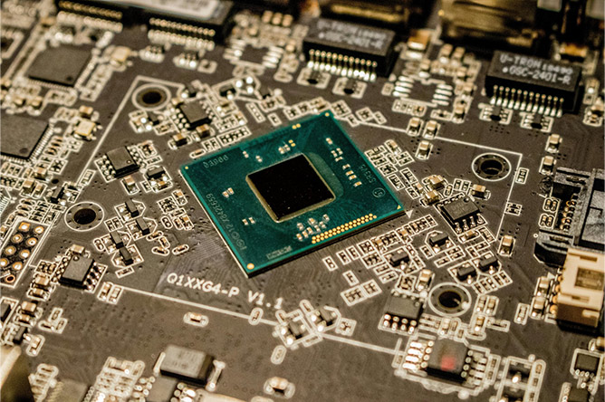
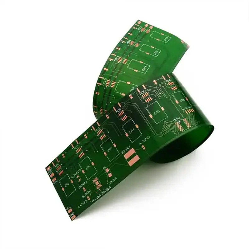
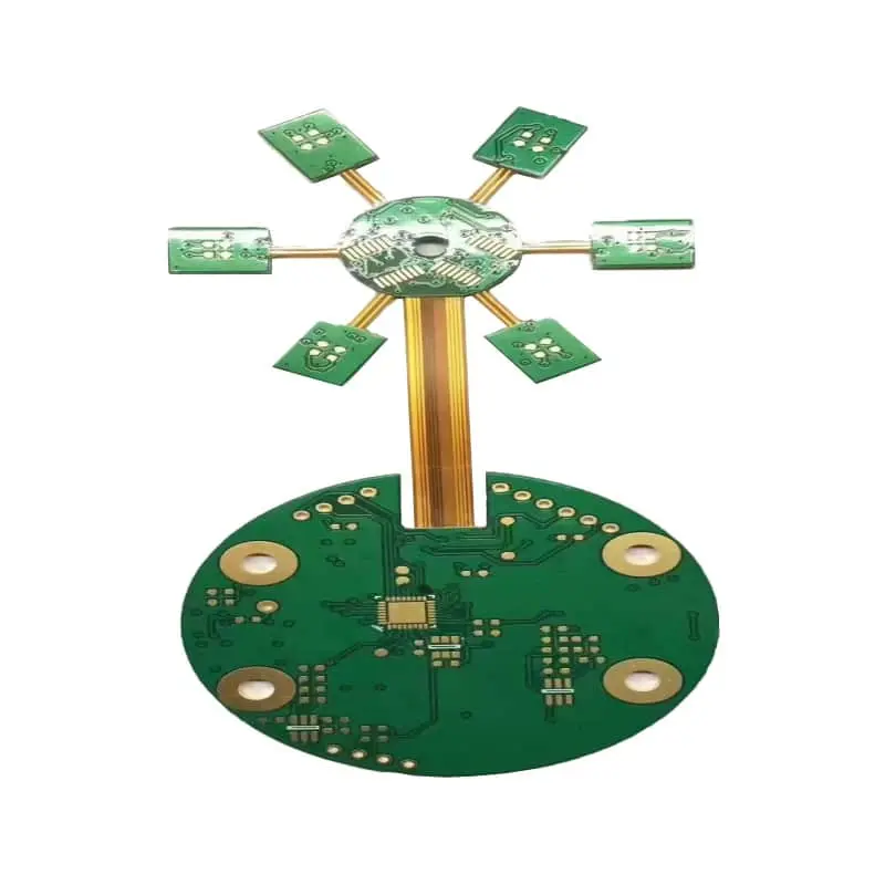
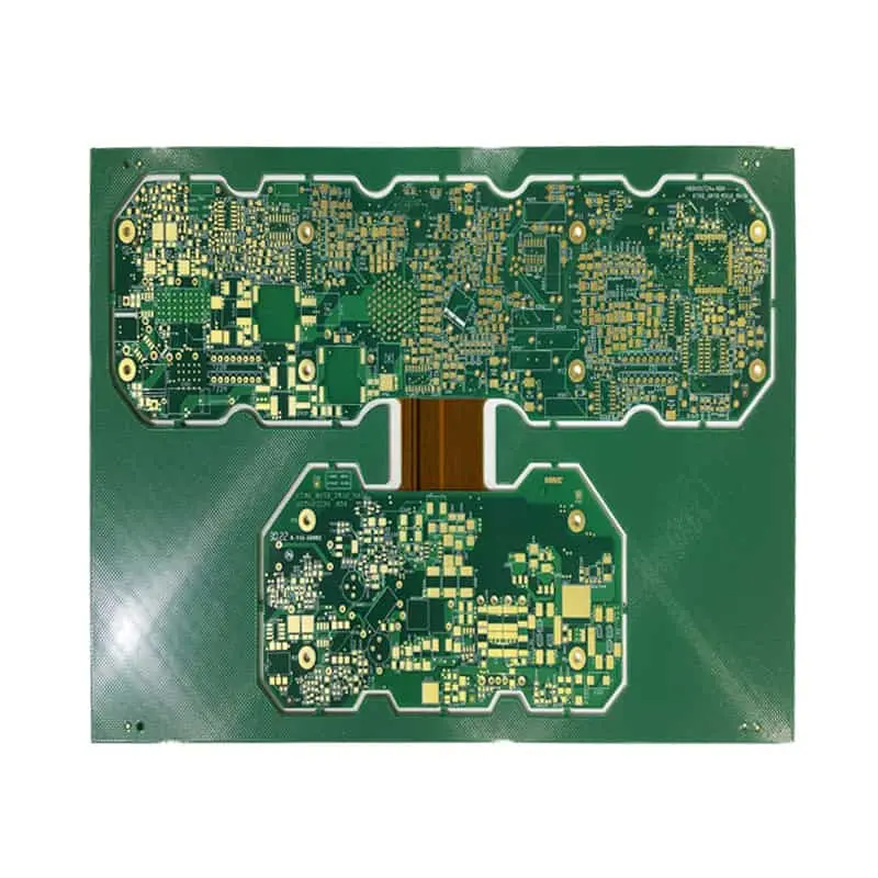
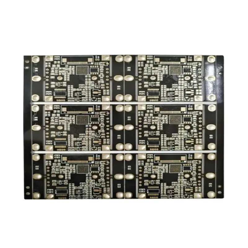
For RF system buyers and design engineers, RF PCB connectors are frequently dismissed as trivial secondary components. In reality, connector‑to‑PCB transitions shape core electrical performance, govern system margin, and can create failures that cannot be fixed with late‑stage debugging, especially as operating frequencies climb higher. Whether you are building 5G communication hardware, defense‑aerospace subsystems, or precision test‑measurement equipment, poor RF PCB connections erode signal integrity, eat into loss budgets, and reduce real‑world system reliability.
Why RF PCB Connections Matter: Signal Integrity, Frequency Range, and Loss
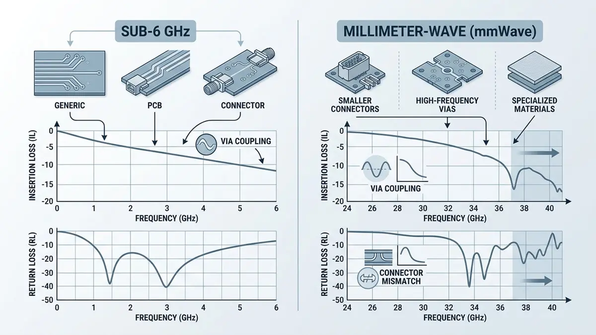
Why RF PCB Connections Matter: Signal Integrity, Frequency Range, and Loss|RF interconnect loss budget visualization for 5G, millimeter‑wave applications
Signal integrity at RF hinges on unbroken impedance continuity across every transition point: connector contacts, PCB vias, solder pads, and transmission‑line segments. Any discontinuity triggers signal reflection, raising return‑loss degradation and insertion‑loss accumulation across your signal chain. The higher your operating frequency, the more severe these effects become. At sub‑6 GHz, minor discontinuities may remain within acceptable performance margins. In millimeter‑wave bands, however, even tiny parasitic gaps or misaligned pads drastically worsen VSWR and add unwanted attenuation, leaving little performance buffer for field operation.
Many competing guides offer generic advice such as “high‑frequency designs require caution”, yet overlook the cumulative loss budget created by the full interconnect chain. Every connector, solder joint, ground via, and cable segment contributes incremental loss that subtracts from your total available system margin. In US‑market 5G base stations, aerospace platforms, and test‑instrument hardware, this margin directly determines operational range, measurement accuracy, and link stability. A small dB penalty from inadequate PCB connections can cause otherwise well‑designed RF hardware to fail compliance or deliver sub‑spec field performance. Tuning software or firmware later cannot compensate for hardware‑level impedance breaks, making upfront connector and transition‑quality decisions non‑negotiable for production‑ready systems.
Impedance Matching, PCB Launch Design, and Layout Constraints
Selecting a high‑performance RF connector delivers limited value without matching PCB launch and footprint design. Real‑world RF performance emerges from treating the connector, pad geometry, anti‑pad clearances, ground vias, and microstrip transition as one unified system, rather than optimizing each element separately. Standard 50‑ohm impedance is the baseline for most microwave hardware; deviations from this target produce reflections that propagate through your full RF path.
Two primary launch architectures dominate board‑level RF work: edge‑launch and cable‑to‑board vertical mounting. Edge‑launch structures excel for high‑frequency millimeter‑wave applications by minimizing mode conversion at the coaxial‑to‑planar transition. Vertical cable‑to‑board connectors save board‑edge real‑estate but demand strict control of anti‑pad size, ground‑via placement, and pad dimensions to suppress parasitic capacitance.
Practical implementation requires actionable design checkpoints. Confirm anti‑pad clearance matches connector vendor recommendations; place sufficient ground vias close to the connector footprint to maintain solid reference ground planes; restrict excess solder bleed‑over that introduces unintended capacitance. US high‑frequency hardware projects commonly face conflicting constraints: tight PCB real‑estate, need for field rework capability, and strict manufacturability rules. Engineers must balance ideal simulated launch performance against fabrication limits. Time‑domain reflectometry (TDR) serves as a powerful validation tool for locating hidden impedance discontinuities within the launch zone before full‑volume production begins.
RF Connector Types Compared: Selection Criteria and Cost‑Performance Trade‑offs
Choosing among RF PCB connectors demands clear evaluation of maximum operating frequency, mechanical footprint, mating durability, power capacity, environmental ruggedness, and total project cost. Raw datasheet parameters alone do not tell the full purchasing story; you must weigh real‑world cost‑performance trade‑offs and supplier consistency risks, particularly for US‑targeted projects requiring formal certification and stable serial production.
- BNC: Low‑cost bayonet‑coupling solution up to approximately 4 GHz. Fast manual mating suits laboratory test setups, though limited frequency capability and weaker vibration performance disqualify BNC for most millimeter‑wave or outdoor deployed hardware.
- N‑Type: Robust threaded connector rated typically to 11 GHz, offering excellent power‑handling and weather resistance. Ideal for outdoor base‑station deployments, yet relatively large footprint makes it unsuitable for compact multi‑channel PCB layouts.
- SMA: Industry‑standard threaded sub‑miniature connector reaching 18 GHz. Balances compact dimensions, reasonable cost, and broad availability for sub‑6 GHz and microwave modules. Note that standard SMA performance degrades rapidly approaching its upper frequency boundary, so avoid pushing it into millimeter‑wave bands.
- SMP / SMPM: Blind‑mate miniature interfaces optimized for dense multi‑channel board stacking. SMPM delivers smaller form‑factor with higher frequency capability, perfect for tightly packed RF modules, but requires precise mechanical alignment and controlled stack‑up tolerances.
- 2.92 mm (K‑type): Air‑dielectric precision connector operating up to 40 GHz, widely used for 5G millimeter‑wave test and measurement.
- 2.4 mm: Extends performance to 50 GHz for V‑band applications.
- 1.85 mm: Premium laboratory‑grade connector supporting 67 GHz for advanced millimeter‑wave research and metrology equipment.
Higher‑frequency precision connectors carry substantially higher unit pricing and tighter assembly tolerances. Your decision workflow should start from system frequency requirements, then available PCB space, mating‑cycle expectations, and environmental exposure. Supplier qualification deserves heavy attention for US projects: inconsistent plating quality or dimensional drift across production lots can invalidate compliance certifications and trigger costly field failures, even if prototype samples pass bench testing.
Reliability, Assembly, EMI Shielding, and Common Failure Modes
Strong bench‑test performance on prototype hardware provides no guarantee of long‑term field reliability. Real‑world RF PCB connector failures arise from combined mechanical, thermal, and environmental stressors, not just electrical specs on a datasheet. Critical factors include mating durability, correct installation torque, soldering or crimp quality, temperature cycling, vibration, humidity exposure, and EMI‑shielding effectiveness.
Improper torque during mating creates one of the most frequent failure sources. Under‑torqued threaded connections produce intermittent contact and drifting VSWR; over‑torque stresses PCB solder pads, initiating invisible micro‑cracks that slowly propagate under vibration and thermal cycles. Eventually pad delamination occurs, causing intermittent or complete RF link dropout — a classic “works‑in‑lab, fails‑in‑field” issue difficult to replicate in short‑duration qualification testing. Soldering process control is equally important: insufficient solder creates weak joints, while excessive solder spills onto signal or ground structures introduces parasitics that degrade high‑frequency response.
For outdoor base‑station, aerospace, and industrial US deployments, environmental ruggedness is paramount. Moisture and corrosion degrade contact resistance; continuous vibration loosens interfaces; repeated thermal cycling fatigues solder joints. EMI shielding performance must also be assessed: poor connector‑to‑board grounding opens leakage paths for RF noise ingress and egress, degrading receiver sensitivity or generating unwanted emissions.
Preventive best‑practices include: enforce documented torque values for each connector series; define soldering profile limits in assembly documentation; specify gold‑plated contacts for high‑reliability service; add environmental screening during component qualification; and document inspection procedures to spot early signs of pad stress before shipment.
Test, Validation, Standards, and Compliance for RF PCB Connections
Robust testing and compliance validation transform subjective connector‑selection choices into auditable engineering decisions, essential for US commercial, defense, and aerospace hardware projects. Many reference materials simply advise “perform testing”, without outlining a practical validation workflow and clear pass‑fail criteria.
Your validation sequence should combine vector‑network‑analyzer (VNA) frequency‑domain measurements alongside TDR time‑domain analysis. Measure insertion loss, return loss, and VSWR across your full operational frequency band to characterize steady‑state electrical performance. TDR helps pinpoint impedance discontinuities localized to connector footprints or launch transitions that frequency‑only measurements may mask. Beyond room‑temperature bench tests, execute environmental qualification: temperature cycling, vibration, humidity, and shock testing to simulate service‑life stress. Apply batch sampling for mass‑production runs rather than relying solely on hand‑picked prototype samples.
Multiple standards frameworks apply to US‑market designs, including IPC PCB manufacturing specifications, MIL‑STD defense qualification requirements, and UL safety standards. Be mindful that project‑specific customer specifications often impose tighter limits than generic industry standards. Document all test reports, measured S‑parameter datasets, and supplier qualification records. This audit trail supports compliance reviews and accelerates troubleshooting if performance anomalies emerge later in product lifecycle.
Next Steps: Move from Specification to Real‑World Application
Armed with knowledge of signal‑integrity risks, PCB‑launch design rules, connector‑family trade‑offs, reliability failure modes, and validation workflows, you are better positioned to avoid expensive redesigns and field‑service events.
Download our full RF PCB Connector Selection Checklist to compare candidate components side‑by‑side against your frequency budget, footprint, environmental, and compliance needs. Submit your application parameters including operating frequency, PCB constraints, mating‑cycle requirements, target market compliance standards, and environmental conditions to receive targeted connector recommendations. You can also request engineering samples and application‑engineering support for your US‑oriented project. We provide supporting compliance documentation and lead‑time estimates aligned with North‑American production timelines to help you de‑risk your RF hardware development cycle.
Frequently Asked Questions
Q: Why do RF PCB connections have a bigger impact on signal integrity at millimeter‑wave frequencies?
A: At millimeter‑wave wavelengths, even tiny mechanical discontinuities and parasitic structures represent meaningful fractions of signal wavelength. Minor impedance breaks create severe reflection and loss, with almost no system margin available to absorb those degradations.
Q: How do I choose between edge‑launch, cable‑to‑board, and vertical RF PCB connectors?
A: Edge‑launch typically delivers superior high‑frequency performance but consumes PCB edge space. Vertical cable‑to‑board variants save edge real‑estate but demand strict launch‑geometry control. Base your choice on maximum operating frequency, available board geometry, and assembly constraints.
Q: What impedance and PCB launch design rules should I follow for an RF connector?
A: Maintain target impedance (most often 50 Ω). Respect vendor‑specified footprint, anti‑pad clearances, and ground‑via placement rules. Avoid excessive solder build‑up, and validate discontinuities using TDR measurements.
Q: How much insertion loss and return loss is acceptable for an RF PCB connection?
A: Acceptable thresholds depend on your overall system loss budget. As general guidance, target return loss better than −20 dB across operational bands for high‑performance designs; evaluate insertion‑loss contribution against your full link budget rather than isolated connector specs.
Q: How do I compare RF connector types such as SMA, SMPM, 2.92 mm, and 2.4 mm on frequency, loss, size, and cost?
A: SMA offers low‑cost compact performance up to 18 GHz. SMPM provides miniature blind‑mate capability for dense stacking. 2.92 mm and 2.4 mm are high‑precision air‑dielectric connectors for millimeter‑wave ranges, with progressively higher frequency capability, tighter tolerances, and increased unit cost.
Q: What causes RF PCB connections to fail in the field, and how can I improve mating durability and environmental ruggedness?
A: Primary root causes include incorrect mating torque, solder‑joint fatigue from vibration and thermal cycling, corrosion, and pad delamination. Mitigate risks by following published torque limits, controlling assembly processes, selecting appropriate plating materials, and completing environmental qualification testing.
Q: What test, compliance, and supplier qualification checks should an RF PCB connector pass before production? A: Complete VNA and TDR electrical characterization, environmental stress screening, and batch‑lot consistency checks. Verify alignment with relevant IPC, MIL‑STD, UL or customer‑specific specifications, and audit supplier manufacturing consistency and documentation capability.
About Author
David Chen LinkedIn Profile
David Chen is a Senior RF/PCB Process Engineer at Shenzhen Hongda Circuit Technology Co., Ltd., with over 12 years of experience in high-frequency PCB fabrication, impedance-controlled stack-up design, and Rogers/PTFE laminate processing. He also boasts an extensive professional background in PCBA manufacturing, PCBA testing, and PCBA optimization, with specialized expertise in high-precision PCBA fault analysis and rigorous PCBA reliability testing. The author has worked with high-layer-count server PCB fabrication, ultra-low-loss backplane stackups, and thermo-mechanical reliability optimization for AI infrastructure projects involving 112G and 224G PAM4 architectures. Skilled in complex circuit design and cutting-edge advanced PCB manufacturing processes, he delivers solutions that elevate product durability and performance across industrial applications. His technical articles focusing on PCBA manufacturing workflows and testing methodologies are widely cited by industry peers and technical platforms, and have gained attention and recognition from industry colleagues.