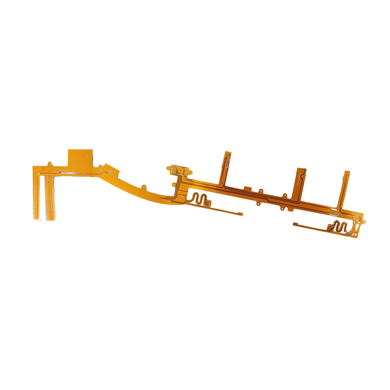
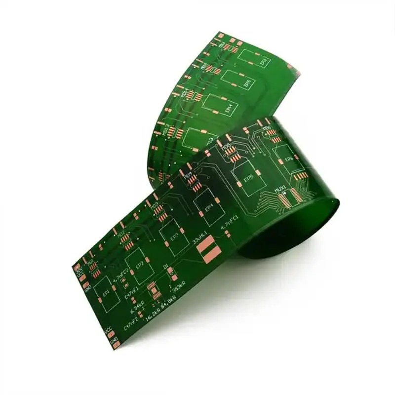
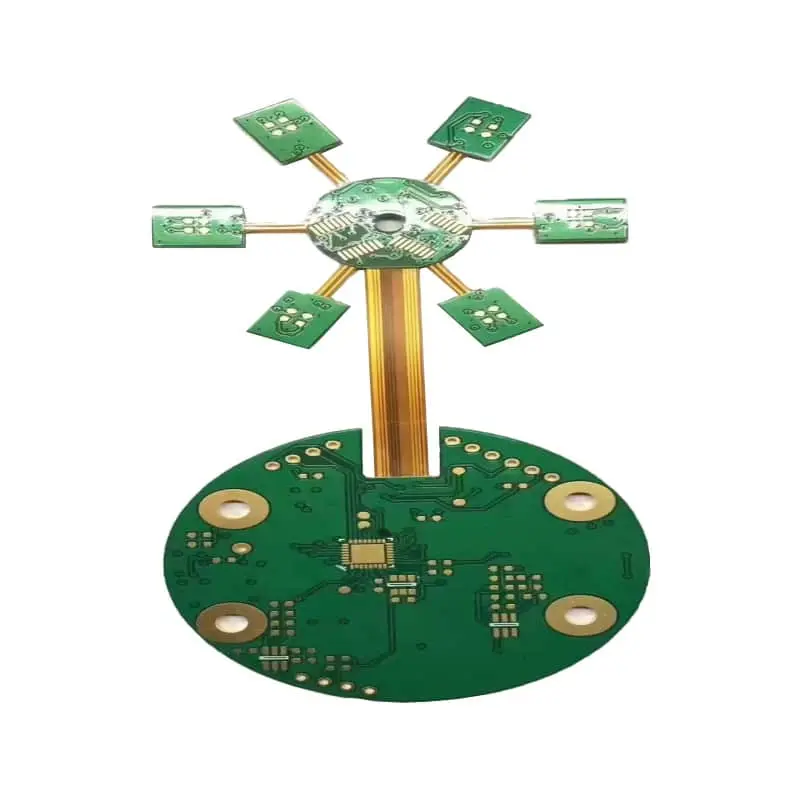
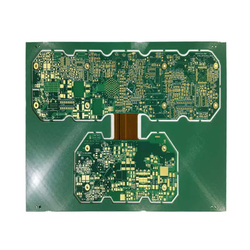
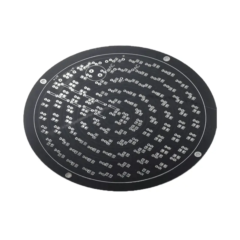
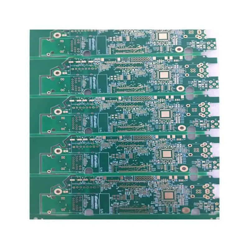
FPC panelization acts as a vital DFM procedure to solve handling difficulties for small flexible circuits, stabilize SMT manufacturing, lower yield loss and manage production costs. Drawing on over 12 years of hands-on experience in PCB and FPC manufacturing engineering, this guide complies with IPC-2223 and IPC-6013 industry standards. It covers panel layout rules, breakaway connecting tab specifications, tear-stop trace design, and minimum dimension requirements for miniature FPC units, helping hardware engineers and procurement buyers avoid common panel design errors before releasing Gerber files.
Introduction
Unlike rigid PCBs, flexible printed circuits cannot adopt conventional V-cut or mouse bite (stamp hole) depaneling solutions. Thin polyimide substrates easily suffer cracking, trace tearing and warpage under the mechanical scoring force generated by V-grooves. For high-volume SMT production, proper panelization is essential, especially for miniature FPCs smaller than 50mm × 50mm.
As a senior PCB manufacturing engineer with more than 12 years of experience in FPC, rigid-flex and high-reliability PCB DFM review and production validation, I have assessed thousands of customer panel designs and supported mass production for consumer, industrial, medical and automotive flex circuit projects. All guidance shared below combines real production yield data with IPC-2223 (Flexible Printed Board Design Standard) and IPC-6013 (Flex Circuit Qualification & Performance Specification), delivering practical, procurement-friendly design rules for OEM hardware teams.
FPC Panelization Core Design Requirements
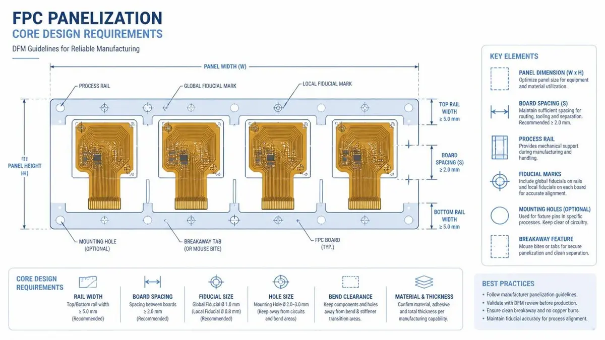
FPC Panelization Core Design Requirements
Recommended Panel Dimensions, Array Layout & Spacing
FPC panels must fit the working range of SMT conveyors, stencil printers and pick-and-place machines.
- Recommended single-unit width: 120mm or 250mm; nesting even quantities of units is preferred for better tooling efficiency and panel utilization.
- Spacing between adjacent FPC units: 2mm by default. For FPC fitted with steel sheet stiffener reinforcement, increase the spacing to 3mm, and keep spacing consistent across the whole array.
- Maximum panel size: 250mm × 600mm; minimum finished panel size for SMT processing: 70mm × 70mm.
- Do not mix different FPC part numbers on one panel. Mixed arrays will interfere with SMT vision alignment, slow down placement speed and bring higher risks of component misloading.
Process Edge, Tooling Holes and Mark Fiducials
A 5mm-wide process border (rail) is required on four sides of the panel unless special instructions are noted in the fabrication order. The process edge holds tooling positioning holes and global fiducial marks for automated SMT alignment.
All process rails need to be included in your Gerber output. If you omit process edges without prior notification to the supplier, your design will likely fail DFM checking and lead to production delays.
Why FPC Panels Do Not Support V-Cut or Mouse Bite
This is one of the most frequent DFM mistakes made by new flex circuit designers. FPC panels rely only on laser routing and breakaway connecting tabs instead of V-cut or stamp holes. The thin polyimide dielectric and rolled-annealed copper traces cannot withstand concentrated mechanical stress from scoring, which creates microcracks that expand during bending or reflow soldering.
The outline of individual units is fully routed, while narrow connecting tabs remain to hold the whole array together through the SMT process. After assembly, operators can separate units by hand-tearing or blade cutting.
Tear Stop Line Design for FPC Panels
What Is a Tear Stop Line?
A tear stop line is a small copper trace added on the signal layer at the root of each breakaway tab. Its core purpose is to stop crack propagation and prevent the split from extending into functional circuit traces during depaneling.
Critical DFM Notes for Tear Stop Implementation
Since tear stop copper traces are placed on the signal layer, you must complete circuit clearance review before adding them. If the copper overlaps existing routing or violates spacing rules, electrical shorts will occur.
If you authorize your PCB manufacturer to add tear stop lines for you, you must leave clear notes on your order and confirm the final production artwork before fabrication starts.
Breakaway Connecting Tab Specification
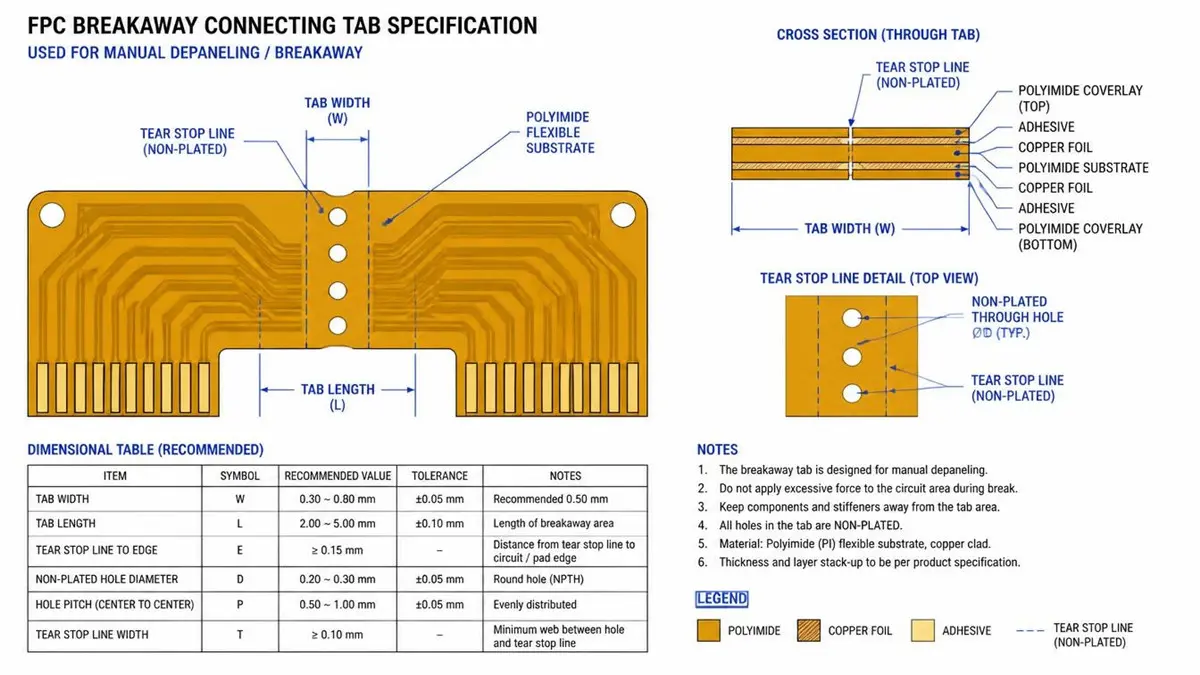
Breakaway connecting tab specification for FPC, different width rules for SMT and non-SMT flexible circuits.
Connecting tab width is decided by three factors: overall panel size, whether SMT assembly is required, and whether steel stiffener or thick FR-4 reinforcement is applied.
- SMT FPC: Standard tab width = 0.8mm. Tabs cannot overlap half-holes or gold finger pads, as these high-precision features will be damaged during separation.
- Non-SMT FPC: Tab width range = 0.25mm ~ 0.3mm. Use 2–3 tabs per unit and mark this requirement in your fabrication notes.
- If you have no special tab requirements, the manufacturer can define the tab layout for you.
Minimum Size Rules for Small FPC Units
Small FPCs bring challenges for automatic conveyor handling, vacuum pickup and stencil printing, so panelization is mandatory for miniature flex circuits.
- FPC with SMT: The minimum finished panel size is 70mm × 70mm. Any single unit smaller than this must be panelized or extended with dummy process edges to reach the 70mm ×70mm minimum panel footprint.
- Single unit below 50mm ×50mm: Panelization is strongly recommended. Irregular-shaped FPC can be submitted for supplier-assisted panel nesting.
- Single unit below 10mm ×10mm: Mandatory panelization or micro-adhesive film carrier shipment. Standalone tiny FPCs cannot run through standard SMT lines without a carrier or panel array.
FAQ for FPC Panelization (Engineer & Procurement Search Intent)
Q1: Can I use V-cut or mouse bite for FPC panel depaneling?
No. FPC is incompatible with V-cut or stamp-hole mouse bite depaneling, according to IPC-2223 flex design guidance. V-cut scoring creates microcracks in polyimide coverlay and copper, which eventually cause open circuits after bending. Laser routing paired with breakaway tabs is the standard singulation method.
Q2: What is the minimum panel size for FPC + SMT assembly?
The minimum finished panel dimension for SMT production is 70mm ×70mm. If your individual FPC unit is smaller, you need to add process rails or nest multiple units into one panel to meet this requirement.
Q3: What tab width should I select for FPC breakaway tabs?
For SMT FPC, use 0.8mm tabs. For bare FPC without assembly, use 0.25–0.3mm tabs with 2–3 tabs per piece. Never place tabs on gold fingers or half-hole pads.
Q4: What is an FPC tear stop line and do I need it?
A tear stop line is a small copper trace at the tab root to stop cracks from spreading into functional circuits during depaneling. It is highly recommended for workflows that use hand-tear depaneling. You must check trace clearance before adding it, as it shares the signal layer.
Q5: What should I do if my FPC unit is smaller than 10mm × 10mm?
FPC units smaller than 10mm × 10mm must be panelized or shipped mounted on micro-adhesive film. Standalone units of this size cannot be reliably handled by standard SMT pick-and-place equipment.
Q6: Can I mix different FPC part numbers on one SMT panel?
It is not recommended. Mixed part panels reduce SMT throughput, increase programming complexity and raise the risk of wrong component placement. For stable production, only identical FPC units should be nested on one panel.
Conclusion
FPC panelization is more than a manufacturing convenience; it is a DFM discipline focused on reliability and cost control, rooted in IPC flex standards. By following the rules for spacing, tabs, tear-stop traces, process edges and minimum sizes above, hardware engineers can reduce DFM revision cycles, cut assembly scrap, and help procurement teams obtain stable, repeatable quotations from FPC suppliers. Always attach your panel notes, tab specifications and tear-stop requirements in your fabrication order to avoid miscommunication.
About Author
David Chen LinkedIn Profile
David Chen is a Senior RF/PCB Process Engineer at Shenzhen Hongda Circuit Technology Co., Ltd., with over 12 years of experience in high-frequency PCB fabrication, impedance-controlled stack-up design, and Rogers/PTFE laminate processing. He also boasts an extensive professional background in PCBA manufacturing, PCBA testing, and PCBA optimization, with specialized expertise in high-precision PCBA fault analysis and rigorous PCBA reliability testing. The author has worked with high-layer-count server PCB fabrication, ultra-low-loss backplane stackups, and thermo-mechanical reliability optimization for AI infrastructure projects involving 112G and 224G PAM4 architectures. Skilled in complex circuit design and cutting-edge advanced PCB manufacturing processes, he delivers solutions that elevate product durability and performance across industrial applications. His technical articles focusing on PCBA manufacturing workflows and testing methodologies are widely cited by industry peers and technical platforms, and have gained attention and recognition from industry colleagues.