Abstract
This page covers custom multilayer PCB manufacturing for hardware engineers and procurement buyers. With over 12 years of hands-on PCB fabrication experience, the author explains stack-up design rules, DFM review, controlled impedance, blind and buried via processing, IPC compliance, quality acceptance criteria, lead time planning and quotation prerequisites. Real yield and failure cases from high-volume industrial and networking projects are included to help buyers reduce re-spins, compare quotes accurately and select a qualified multilayer PCB supplier. Keywords: custom multilayer PCB manufacturing, multilayer PCB fabrication, controlled impedance PCB, blind and buried via PCB, IPC-6012 PCB, PCB DFM review
I am a senior PCB manufacturing engineer with more than 12 years of production, process and quality engineering experience in rigid multilayer PCB fabrication. I have led hundreds of NPI prototype runs and mass production lots for industrial control, automotive, networking and high-speed communication boards, following IPC-2221C, IPC-2222B and IPC-6012D standards daily. This practical guide is written for hardware engineers and procurement specialists who need reliable multilayer PCB manufacturing without hidden yield risks.
What is custom multilayer PCB manufacturing and when do you need it?
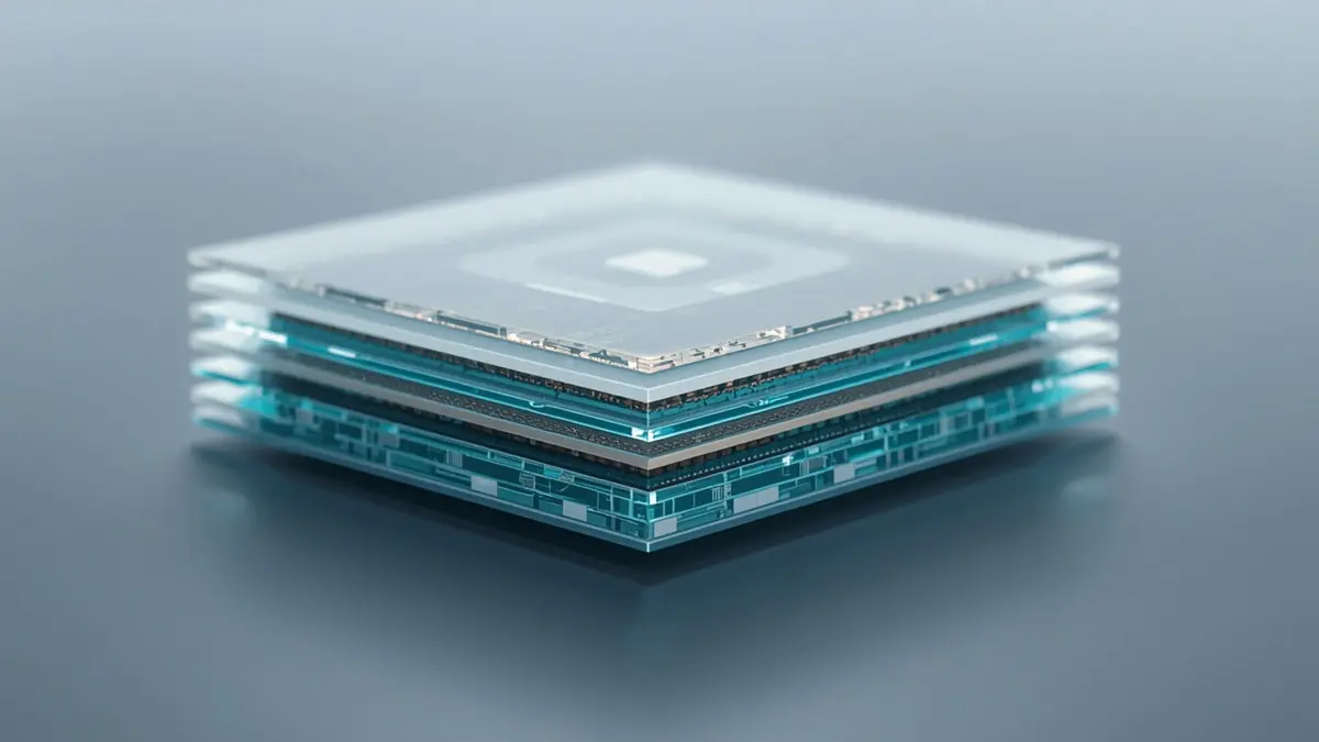
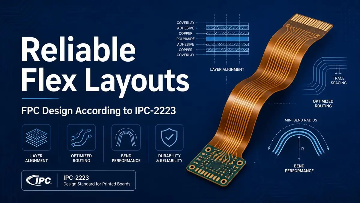
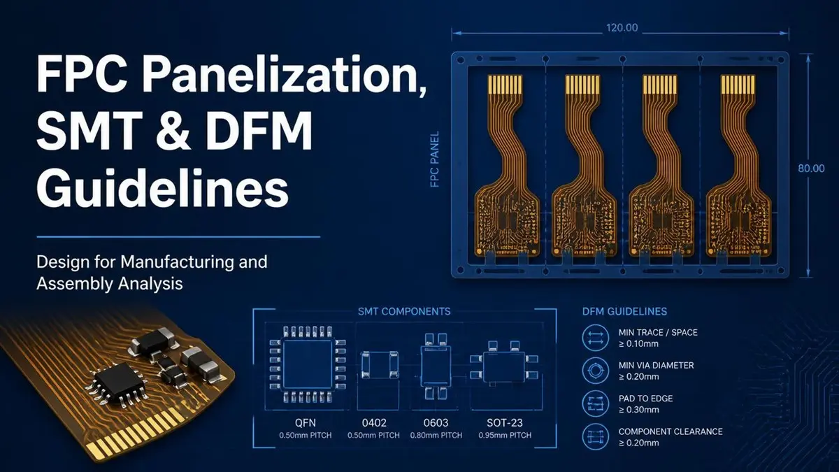
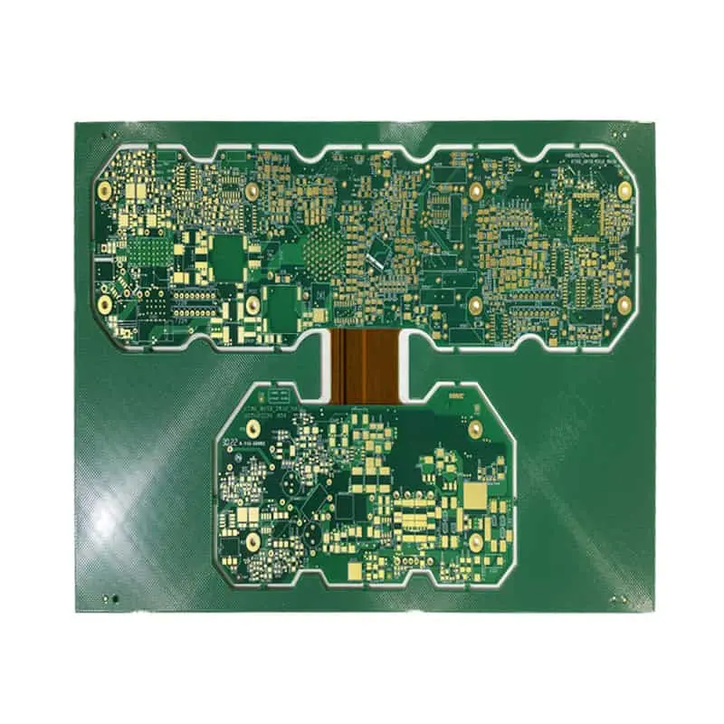
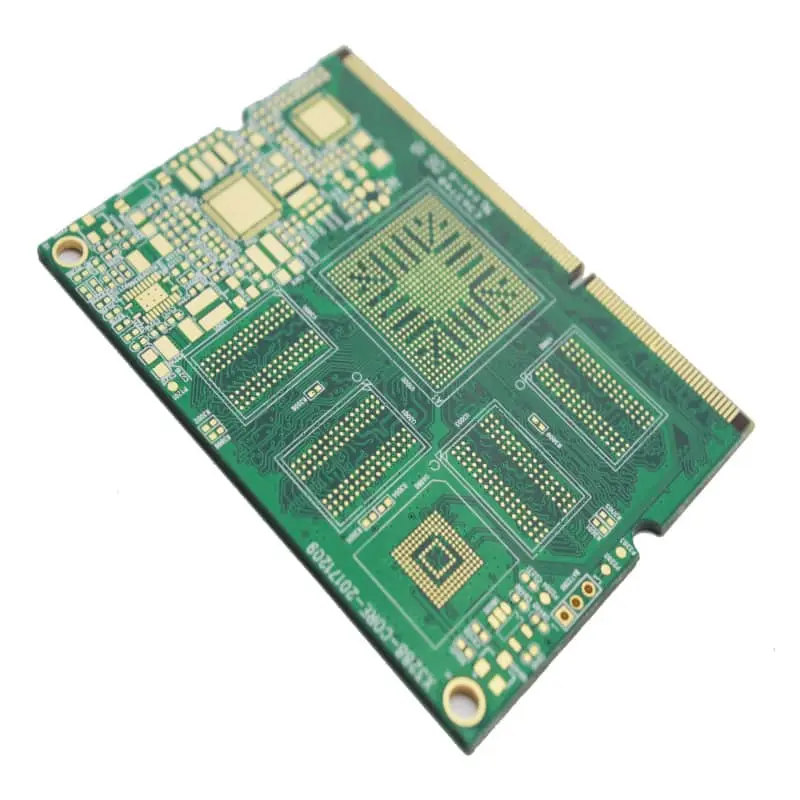
Cross-section visualization of custom multilayer PCB stack-up, showing core copper layers and prepreg dielectric structure for controlled impedance and blind/buried via designs
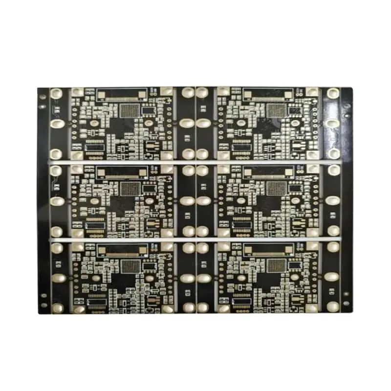
Custom multilayer PCB manufacturing builds rigid printed circuit boards with three or more conductive copper layers laminated together with prepreg and core materials. Unlike simple double-sided boards, multilayer structures separate power planes, ground planes and high-speed signal traces to improve noise isolation, power integrity and routing density.
Typical applications that require multilayer PCB fabrication
Multilayer PCBs are standard for designs that cannot fit on 2-layer or 4-layer boards. Common use cases include industrial controllers, AI accelerator boards, router and CPE hardware, automotive electronics, medical diagnostic modules and high-speed PCIe signal boards.
Core technical constraints of multilayer PCB manufacturing
The main manufacturing limits are minimum layer count, core thickness, prepreg resin flow, copper weight, annular ring tolerance, registration alignment and resin recession around microvias. Many low-cost fabs accept Gerber files but lack stable lamination control, which causes layer shift, impedance drift and inner-layer shorting during mass production. I have seen multiple customer projects where poor lamination alignment created 15–25% scrap rate in the first production run, even after a passing prototype.
What stack-up and material choices affect multilayer PCB yield and cost?
Stack-up design is the single most important input for predictable multilayer PCB manufacturing. A poor stack-up will force higher material cost, tighter tolerance control and longer lead time, or simply fail impedance testing.
Standard FR-4, high-Tg FR-4 and high-frequency laminate tradeoffs
Standard FR-4 works for most low-speed industrial multilayer boards. High-Tg FR-4 (Tg 170°C or higher) is required for reflow thermal cycling and automotive environments. High-frequency materials such as PTFE or hydrocarbon laminates are used for RF and microwave signal layers, but these materials have different lamination cycles and drilling parameters, and they cannot be mixed with standard FR-4 without careful process validation.
How prepreg resin content impacts impedance stability
Resin flow during lamination changes the dielectric thickness between signal layers, directly shifting differential impedance. For controlled impedance multilayer PCBs, we lock the prepreg style, resin percentage and lamination cycle in the CAM package before tooling. I always recommend engineers avoid “generic prepreg” when impedance tolerance is ±5% or tighter.
What DFM checks are mandatory before multilayer PCB fabrication release?
DFM review for multilayer boards is far more complex than 2-layer PCB DFM. Inner-layer clearance, copper balancing, copper density, anti-pad size and thermal relief must all be reviewed before CAM output.
Inner-layer DFM rules for blind and buried via PCB
Blind vias connect outer layers to selected inner layers; buried vias connect inner layers only. These structures require sequential lamination, which adds process steps and cost. The most common DFM violation I catch in customer files is insufficient anti-pad clearance on buried via layers, which creates hidden inner-layer shorts that pass AOI but fail electrical test.
Copper balancing and panel warpage control
Unbalanced copper distribution between top and bottom sides or between adjacent inner layers causes board warpage after lamination. Warped multilayer PCBs will fail SMT assembly, especially for BGA and QFN packages. Our standard DFM checklist includes copper density balancing and panel support coupons per IPC-2221C guidance.
What quality standards apply to multilayer PCB inspection and acceptance?
We follow IPC-6012D for rigid multilayer PCB performance specifications and IPC-A-600G for visual acceptance criteria. Buyers must specify IPC Class 2 or Class 3 on the RFQ, because acceptance tolerances change dramatically between these two classes.
IPC Class 2 vs Class 3 multilayer PCB requirements
IPC Class 2 is general electronic product grade, allowing minor cosmetic defects that do not impact reliability. IPC Class 3 is high-reliability grade for automotive, medical and aerospace electronics, with tighter annular ring, registration, plating and void limits. If you order Class 3 boards without stating it in the quote, the supplier will default to Class 2 and the boards will not pass your final quality audit.
Electrical test, AOI and impedance verification
All bare multilayer boards go through netlist continuity and isolation electrical test. AOI inspects outer-layer features after exposure and etching. Controlled impedance testing is a separate measurement using impedance test coupons; standard flying probe E-test does not verify impedance values.
What documents do you need to submit for a multilayer PCB RFQ?
Many delayed quotes and miscommunication happen because buyers send incomplete files. A complete RFQ package reduces DFM clarification cycles and gives you comparable pricing from different fabs.
Mandatory files for multilayer PCB quotation
Gerber or ODB++ files, drill file, layer stack-up drawing, impedance requirements with target and tolerance, surface finish specification, copper weight, board thickness, panelization note, IPC class and quantity breakdown (prototype / pilot / mass production).
Information that helps shorten lead time
If you have approved material part numbers, preferred surface finish, special test requirements (impedance report, cross-section, thermal cycling sample) and target ship date, include these in the first RFQ. This avoids rework after tooling starts.
How do lead time, MOQ and pricing work for custom multilayer PCB manufacturing?
Pricing is not driven only by board area. Layer count, minimum line width and spacing, blind/buried vias, controlled impedance, material grade, surface finish and order volume all change unit price.
Prototype lead time vs mass production lead time
Prototype multilayer PCB orders use dedicated rapid CAM and small batch panels. Mass production requires material stocking, lamination batch scheduling and full quality sampling. A 6-layer prototype may ship in 7–10 working days, while the same design in mass production can take 18–25 working days, depending on laminate availability.
Non-recurring engineering (NRE) and tooling charges
NRE includes CAM engineering, tooling, drill files and panel setup. NRE is usually one-time per Gerber revision. When comparing quotes, separate NRE, stencil, test coupon, special process fees and unit price. A low unit price quote may hide expensive extra charges for impedance testing or sequential lamination.
Frequently Asked Questions for Multilayer PCB Buyers and Hardware Engineers
- What is the difference between IPC Class 2 and Class 3 multilayer PCB? IPC Class 2 is for general electronic products with standard reliability; Class 3 is high-reliability for automotive, medical and mission-critical hardware. Class 3 applies tighter limits on registration, plating voids, annular ring and cosmetic defects, and it raises both manufacturing cost and inspection sampling frequency.
- Can a multilayer PCB supplier guarantee controlled impedance without stack-up confirmation? No. Controlled impedance depends on core thickness, prepreg dielectric constant, copper thickness and trace width. A valid impedance guarantee requires a locked stack-up and material specification before production. Without stack-up approval, impedance drift is common and not covered by standard quality claims.
- What causes layer shift in multilayer PCB manufacturing? Layer shift mainly comes from inaccurate inner-layer registration, unstable lamination pressure and temperature cycles, poor panel tooling and uneven prepreg resin flow. The risk rises sharply with blind and buried via sequential lamination. A qualified fab will use registration targets and verify layer alignment by cross-section sampling.
- Which surface finish is best for multilayer PCB with BGA and high-speed traces? ENIG (immersion gold) is the most common choice for BGA and fine-pitch SMT because it delivers flat, coplanar pads. OSP is low-cost but has limited shelf life and is not suitable for multiple reflow cycles. HASL is low-cost but poor for fine pitch and high-speed impedance consistency.
- What files are required to get an accurate multilayer PCB quote? You need Gerber/ODB++, drill files, stack-up drawing, impedance requirements, copper weight, board thickness, surface finish, IPC class, quantity tiers and any special test requirements such as cross-section or impedance report.
- How can I reduce multilayer PCB cost without sacrificing reliability? Optimize layer count, relax impedance tolerance where possible, use standard FR-4 instead of high-frequency laminates, avoid unnecessary blind/buried vias, balance copper density to reduce warpage scrap, and group orders into larger panels. Never reduce cost by downgrading IPC class or removing critical test coupons.
Ready to send your multilayer PCB RFQ?
Share your Gerber or ODB++ files, stack-up and specifications with our engineering team. We complete a formal DFM review, flag yield risks, confirm IPC acceptance class and deliver a clear quote separated by NRE, unit price and special process charges. Our team supports prototype, pilot and volume multilayer PCB manufacturing for industrial, networking and automotive projects.
About Author
David Chen LinkedIn Profile
David Chen is a Senior RF/PCB Process Engineer at Shenzhen Hongda Circuit Technology Co., Ltd., with over 12 years of experience in high-frequency PCB fabrication, impedance-controlled stack-up design, and Rogers/PTFE laminate processing. He also boasts an extensive professional background in PCBA manufacturing, PCBA testing, and PCBA optimization, with specialized expertise in high-precision PCBA fault analysis and rigorous PCBA reliability testing. The author has worked with high-layer-count server PCB fabrication, ultra-low-loss backplane stackups, and thermo-mechanical reliability optimization for AI infrastructure projects involving 112G and 224G PAM4 architectures. Skilled in complex circuit design and cutting-edge advanced PCB manufacturing processes, he delivers solutions that elevate product durability and performance across industrial applications. His technical articles focusing on PCBA manufacturing workflows and testing methodologies are widely cited by industry peers and technical platforms, and have gained attention and recognition from industry colleagues.