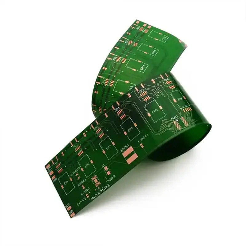
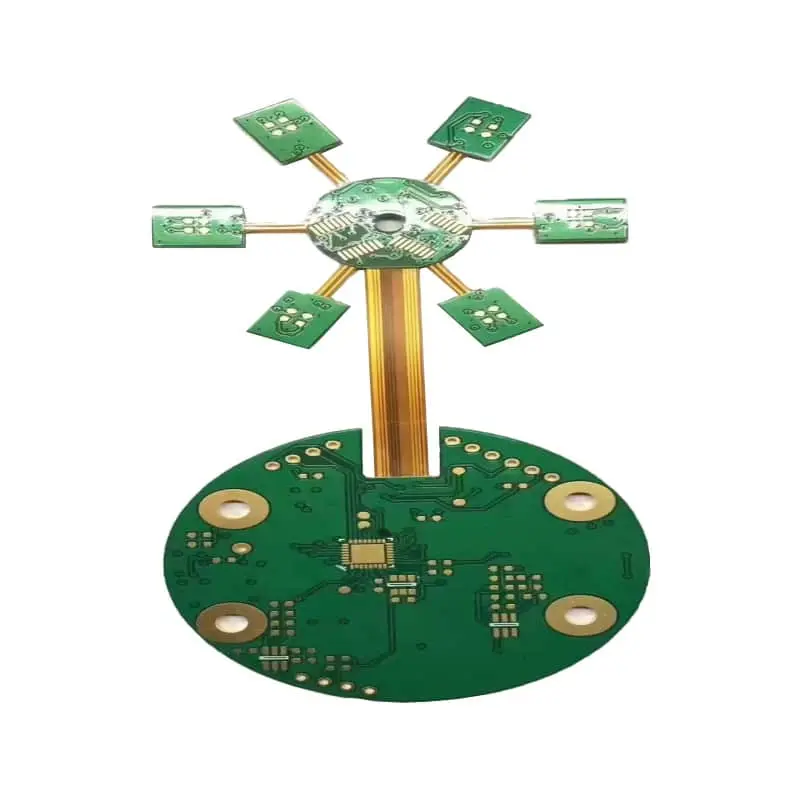
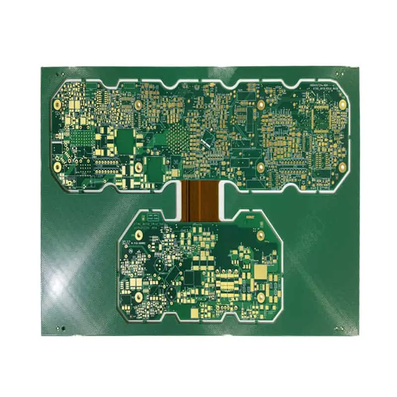
Copper clad laminate for multilayer PCB directly defines multilayer printed‑circuit‑board performance, as final board capability is fundamentally bounded by CCL and prepreg material choices. Even well‑optimized stackups and precise layout will deliver inconsistent yields, signal integrity failures, or thermal‑reliability issues if base materials, lamination workflows, and quality benchmarks are mis‑specified. This practical buying guide walks through material selection, manufacturing workflow, lamination process windows, IPC‑aligned quality control, cost drivers, and supplier qualification to help you write unambiguous purchase requirements and avoid costly field failures.
Materials Selection: Resin Systems, Glass Fabric, and Copper Foil for Multilayer Boards
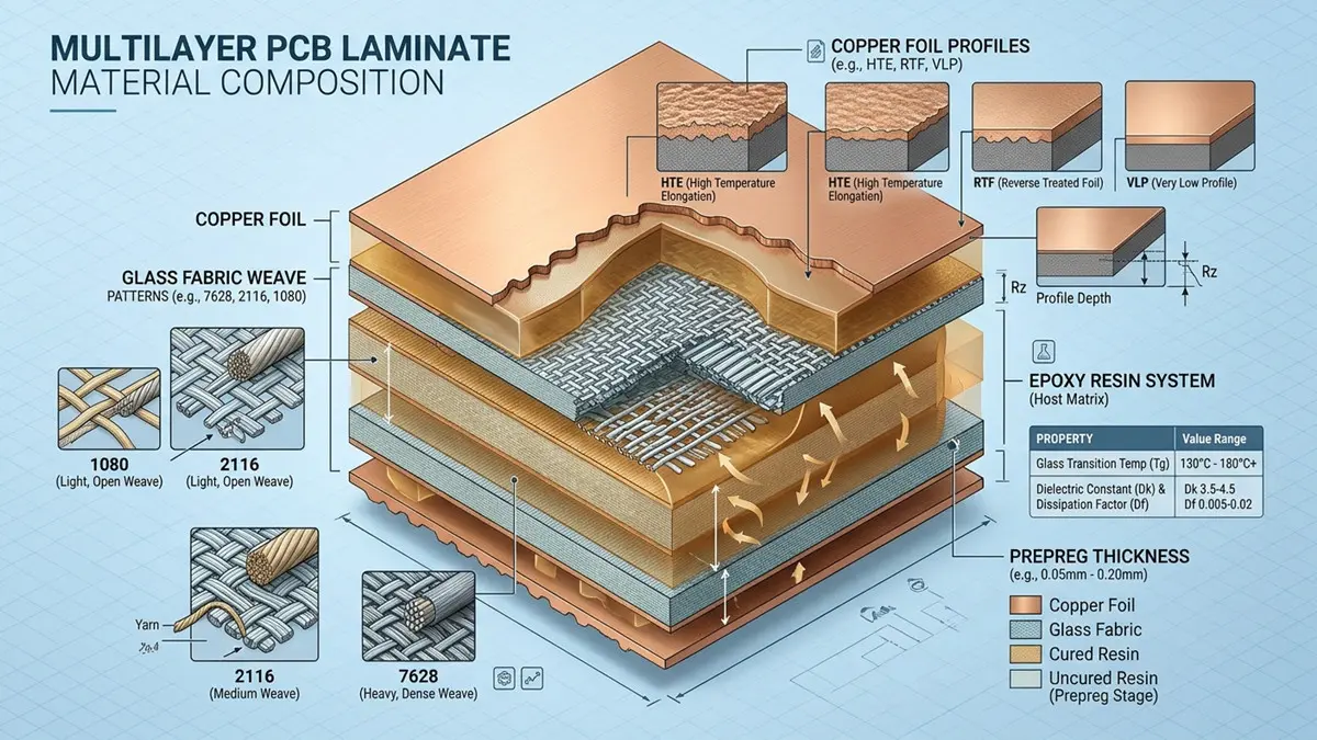
Multilayer PCB Laminate Material Composition and Technical Specifications Diagram
Material specifications set the upper limit for finished‑board performance; procurement teams must evaluate resin chemistry, glass‑fabric weave, and copper‑foil grades in parallel rather than only ordering generic “FR‑4” or “high‑frequency laminate”.
Resin‑system trade‑offs dominate lead‑free multilayer reliability. High‑Tg epoxy improves thermal resistance and reduces Z‑axis expansion yet can narrow the manufacturing processing window. Halogen‑free formulations meet environmental mandates but typically show higher moisture absorption and higher cost versus conventional brominated FR‑4. Engineers must balance Tg, water absorption, reflow survivability, process latitude, and total landed cost when selecting resin families. Tuning Dk/Df for high‑speed designs requires matching resin chemistry and glass‑fabric resin content rather than selecting only by datasheet nominal values.
Glass‑fabric styles directly govern cured dielectric thickness and resin flow. Common weave styles include 7628 for thicker core dielectrics, 2116 for general‑purpose multilayers, and 1080 for thin HDI stack‑ups. Each weave delivers distinct resin‑content ranges and final pressed thickness (reported in mil with mm conversion: 1 mil = 0.0254 mm). Low resin‑content fabrics risk resin starvation around large copper planes; high resin content improves fill but increases resin bleed‑out risk during pressing. Gel‑time values determine how quickly resin cross‑links, dictating how much time remains for gap‑filling before gelation occurs.
Copper‑foil selection impacts signal integrity, etch‑factor, and interlayer peel strength. HTE, RTF, VLP, and rolled‑annealed foils each carry trade‑offs for high‑frequency loss and inner‑layer adhesion. Copper thickness is specified in ounces (½ oz, 1 oz; 1 oz ≈ 35 µm). Surface preparation via brown‑oxide or black‑oxide roughening creates micro‑texture that raises mechanical peel strength between prepreg and inner‑layer copper features.
Use this high‑level selection matrix for supplier conversations:
| Application | Resin Family | Glass Style | Foil Recommendation |
|---|---|---|---|
| Standard multilayer | Mid‑Tg FR‑4 | 7628 / 2116 | HTE ½–1 oz |
| Lead‑free high‑reliability | High‑Tg halogen‑free | 2116 / 1080 | RTF |
| High‑speed HDI | Low‑Dk epoxy | 1080 | VLP / rolled copper |
When releasing purchasing documents, reference IPC‑4101 slash‑sheet numbers alongside performance targets rather than only commercial product names.
Step‑by‑Step Fabrication Flow: From Prepreg Treating to a Pressed Multilayer Panel
Understanding factory workflow helps buyers spot gaps in supplier capability and write tighter acceptance criteria. The production sequence starts with resin mixing and treating: liquid epoxy resin is coated onto woven glass fabric on a treater line to produce B‑stage prepreg sheets. Prepreg is then sheared to panel size, matching finished‑panel dimensions.
Inner‑layer cores go through imaging, etching, and oxide‑treatment (brown or black oxidation) before stack‑up. Multilayer assembly follows build‑up sequence rules for sequential lamination when blind‑buried vias are required. Registration is maintained via pin‑tooling or hot rivet fastening to mitigate layer‑shift risk; blind‑via constructions demand tighter registration tolerances than simple non‑sequential multilayers.
During lay‑up (“book assembly”), materials are stacked in exact order: mirror plate, release film, cushion padding, copper foil, prepreg sheets, processed inner‑layer cores, additional prepreg, outer‑layer copper foil, more cushion media, and final steel plate. Each auxiliary material fulfills a defined function: release film prevents sticking to steel plates, cushion pads distribute pressure evenly to reduce copper wrinkling and thickness variation. Prepreg orientation and stacking sequence strongly influence resin flow and cavity filling around copper features.
After book assembly, panels move into the vacuum press. Lamination parameters (temperature, pressure, vacuum) are covered in the next section. Post‑press operations include panel de‑stacking, cooling, edge routing / milling, and initial dimensional inspection. This sequence applies for both conventional multi‑layer and HDI sequential‑build‑up structures.
Lamination Process Window: Temperature Ramp, Pressure, Vacuum, and Cure Cycle
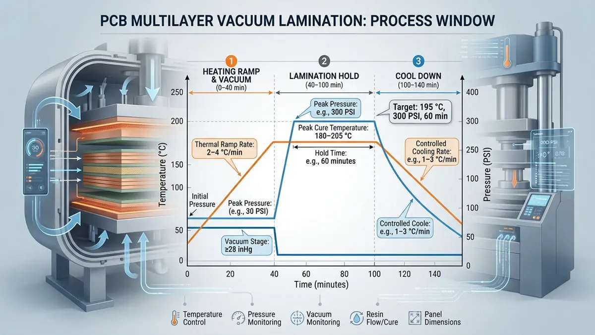
PCB Multilayer Vacuum Lamination Process Window: Temperature and Pressure Cure Cycle Graph
The lamination process window defines acceptable operating bounds to achieve full resin cure, adequate resin flow, minimal voiding, and uniform panel thickness. All temperature values are given in °C with °F reference for North‑American press equipment readouts生益科技.
Typical heat‑up ramp rates range from 2–4 °C/min (3.6–7.2 °F/min) through the critical 80 °C‑140 °C zone where resin softens and begins to flow. Vacuum should pull to ≥28 inHg before significant resin gelation to evacuate trapped air and suppress void formation. Staged pressure is standard: low initial pressure while resin flows, followed by full hydraulic pressure once material temperature reaches 80‑100 °C. Peak curing temperatures differ by material grade: standard FR‑4 cures near 180‑190 °C (356‑374 °F); high‑Tg halogen‑free materials often require 190‑205 °C (374‑401 °F) to reach sufficient cure‑index values. Hold‑time at peak temperature must increase for thicker books or larger panel formats.
Resin‑flow management is central to quality outcomes. Prepreg resin content, gel‑time, volatile fraction, and cold‑storage / conditioning history jointly determine whether resin fills copper gaps without excessive squeeze‑out. If resin flows too fast, resin starvation occurs over large copper areas; if gel‑time is too short, insufficient fill creates micro‑voids, lowering peel strength and increasing thickness non‑uniformity. Prepreg removed from frozen storage must complete full room‑temperature conditioning before lay‑up to avoid condensation‑driven defects.
| Material Grade | Ramp Rate | Cure Temperature | Typical Hold Time |
|---|---|---|---|
| Standard FR‑4 | 2‑3 °C/min | 180‑190 °C (356‑374 °F) | 60‑90 min |
| High‑Tg Halogen‑Free | 2‑3.5 °C/min | 190‑205 °C (374‑401 °F) | 90‑120 min |
Cool‑down rates also affect warpage; controlled cooling below Tg minimizes panel bow and twist.
Quality Control, Test Standards, and Defect Troubleshooting
Validating CCL and finished multilayers relies on the IPC‑4101 (base laminate specification), IPC‑6012 (rigid printed‑board performance), and IPC‑TM‑650 (test‑method protocols) standards framework, the baseline for US‑market acceptance testing.
Key measurable parameters include peel strength (lb/in), glass‑transition temperature Tg measured via DSC, TMA or DMA (results can diverge across test techniques), Dk/Df measured via SPDR fixture, thermal‑stress resistance, dimensional stability, and warpage / twist limits per IPC‑6012 Class 2 or Class 3. When preparing purchase specifications, always state both target value and acceptance tolerance together with required test‑method references.
Common press‑related defects with root‑cause and corrective guidance are summarized below:
| Defect | Primary Causes | Corrective Actions |
|---|---|---|
| Voids | Insufficient vacuum, trapped moisture, fast gel‑time | Improve vacuum hold; bake cores/prepreg; review prepreg shelf‑life |
| Resin Starvation | Low resin‑content prepreg, excessive pressure | Select higher‑resin‑content prepreg; optimize pressure ramp |
| Delamination | Moisture absorption, incomplete cure, contaminated inner‑layers | Strict prepreg conditioning; verify cure index; enforce inner‑layer cleanliness |
| White Edges | Edge moisture ingress, poor sealing of press‑book | Seal panel edges; control factory humidity |
| Copper Foil Wrinkling | Uneven pressure distribution, inadequate cushion material | Check cushion pad condition; verify book stacking |
| Panel Warpage | Unbalanced copper distribution, rapid cool‑down, mismatched Tg | Enforce balanced stack‑up; implement controlled cool‑down profile |
| Blind‑Hole Mis‑registration | Tooling drift, material shrinkage | Use pinned fixtures; apply compensation scaling for sequential lamination |
C‑SAM acoustic scanning identifies hidden internal voids and delamination non‑destructively. Always define Class 2 / Class 3 void‑area limits in your procurement documents rather than relying on informal verbal agreements.
Cost per Square Meter, Supplier Vetting, and Domestic vs Imported Materials
CCL pricing scales with resin performance grade, Tg classification, copper‑foil type, glass‑fabric selection, panel dimensions, order volume, and layer‑count complexity. Budget ranges can be quoted per square meter and converted to US customary USD per square foot (1 m² ≈ 10.764 sq ft). Standard FR‑4 sits at the lower end; high‑Tg halogen‑free and low‑loss high‑speed materials command significant premiums. Larger batch sizes reduce unit cost while prototype small‑lot orders carry higher per‑unit overhead.
Sourcing teams must weigh imported‑material benefits against tariff exposure, ocean‑transit lead‑times, and batch‑to‑batch consistency risk. Local stock can compress lead‑time for urgent projects even with slightly higher unit price.
Effective supplier qualification is more than checking brand names; use these actionable screening criteria: valid UL recognition, correct IPC‑4101 slash‑sheet documentation, accessible local inventory, responsive application‑engineering support, and demonstrated fast‑turn sampling capability.
Incoming‑material control directly improves downstream yield: perform incoming dimensional and visual checks, enforce cold‑chain storage for sensitive prepreg, allow adequate warm‑up / conditioning time after freezer removal, and strictly follow FIFO inventory rotation against prepreg expiry dates. Many avoidable lamination defects originate in poor receiving and material‑handling rather than press‑program errors.
Next Steps & Call‑to‑Action
Turn technical requirements into actionable quotes with three clear next‑step options: submit your full stack‑up drawing to receive formal CCL and prepreg pricing, download our material‑selection plus incoming‑inspection checklist for your procurement workflow, or book a complimentary engineering review session.
Share your key parameters: target layer‑count, Tg requirement, copper‑weight specification, finished panel dimensions, reliability class (IPC‑6012 Class 2 / 3), and required lead‑time, and we will return a manufacturable stack‑up recommendation together with itemized pricing. Our North‑America‑based technical support delivers fast response for design questions and prototype turn‑around to keep your projects on schedule.
Frequently Asked Questions
Q: What is the difference between a copper‑clad laminate and a prepreg in multilayer‑board fabrication? A: CCL (copper‑clad laminate) is a fully‑cured dielectric core with copper foil permanently bonded to one or both sides. Prepreg is partially‑cured B‑stage glass‑epoxy sheet that melts, flows, and cross‑links during lamination to bond multiple cores together in multilayer assemblies.
Q: What lamination temperature, pressure, and cure time are typical for FR‑4 multilayer boards? A: Standard FR‑4 generally ramps 2‑3 °C/min, full pressure ~250‑350 PSI, cure temperature 180‑190 °C with 60‑90 min hold at peak temperature under high‑vacuum press conditions; exact values depend on prepreg datasheet and total book thickness.
Q: Which copper‑foil type should I choose for high‑frequency or high‑density multilayer PCBs? A: VLP or rolled low‑profile copper minimizes conductor‑loss for high‑frequency signal paths; RTF balances cost, peel‑strength and roughness for general‑purpose HDI. HTE is cost‑effective for non‑high‑speed designs.
Q: How do you prevent voids, resin starvation, and delamination during CCL pressing? A: Maintain deep vacuum before resin gelation; select matching resin‑content prepreg; strictly condition cold‑stored materials; bake‑out absorbed moisture; control ramp‑and‑pressure profiles; keep inner‑layer surfaces clean and free of contamination.
Q: Which IPC standards apply to copper‑clad‑laminate and multilayer‑board qualification? A: IPC‑4101 defines base‑laminate specifications; IPC‑6012 sets finished‑rigid‑board acceptance criteria; IPC‑TM‑650 contains all relevant physical and electrical test‑method procedures.
Q: How much does copper‑clad laminate cost per square meter, and what drives the price? A: Cost rises with higher‑performance resin systems (high‑Tg, halogen‑free, low‑Dk/Df), premium copper foils, smaller lot‑sizes, special panel dimensions. Imported materials add tariff and freight‑related variables.
Q: What causes warpage in multilayer boards, and how is dimensional stability controlled? A: Primary causes are electrically‑unbalanced copper weight top‑to‑bottom, mismatched‑CTE materials, and overly‑fast cooling after pressing. Control by enforcing symmetric stack‑up design, matching material families, and implementing slow controlled cool‑down cycles in the press.
About Author
David Chen LinkedIn Profile
David Chen is a Senior RF/PCB Process Engineer at HAODA ELECTRONIC CO.,LIMITED with over 12 years of experience in high-frequency PCB fabrication, impedance-controlled stack-up design, and Rogers/PTFE laminate processing. He also boasts an extensive professional background in PCBA manufacturing, PCBA testing, and PCBA optimization, with specialized expertise in high-precision PCBA fault analysis and rigorous PCBA reliability testing. The author has worked with high-layer-count server PCB fabrication, ultra-low-loss backplane stackups, and thermo-mechanical reliability optimization for AI infrastructure projects involving 112G and 224G PAM4 architectures. Skilled in complex circuit design and cutting-edge advanced PCB manufacturing processes, he delivers solutions that elevate product durability and performance across industrial applications. His technical articles focusing on PCBA manufacturing workflows and testing methodologies are widely cited by industry peers and technical platforms, and have gained attention and recognition from industry colleagues.