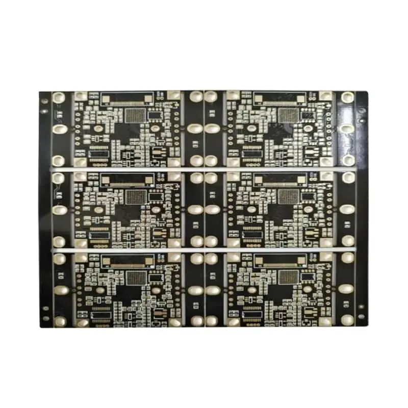
PCB phototool negative‑film deformation creates common production headaches for every PCB shop: unexpected registration drift, annular‑ring offset, and frustrating batch‑to‑batch inconsistency. Many manufacturing teams misdiagnose these defects as faulty dry‑film or photoplotting mistakes. As a result, they waste valuable materials, labor hours and delivery lead‑time while troubleshooting incorrect root causes. For procurement and production managers, sourcing suitable phototool film represents only part of the fix. Consistent, reliable PCB output also relies on well‑calibrated environmental controls, standardized inspection workflows, precise measurement compensation, and balanced equipment trade‑offs. This practical guide supports US‑based PCB fabricators to cut rework rates, improve first‑pass yield, and make well‑informed purchasing choices for phototool consumables and imaging hardware.
Root Causes: Why PCB Negative Films Stretch, Shrink, and Lose Registration
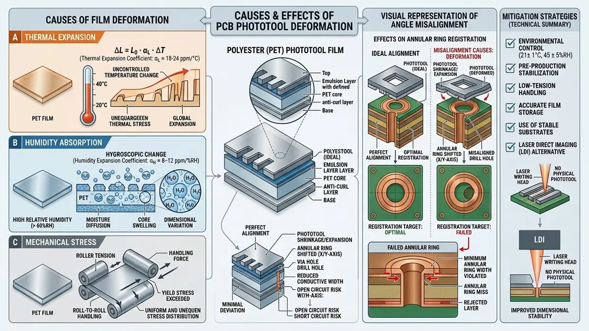
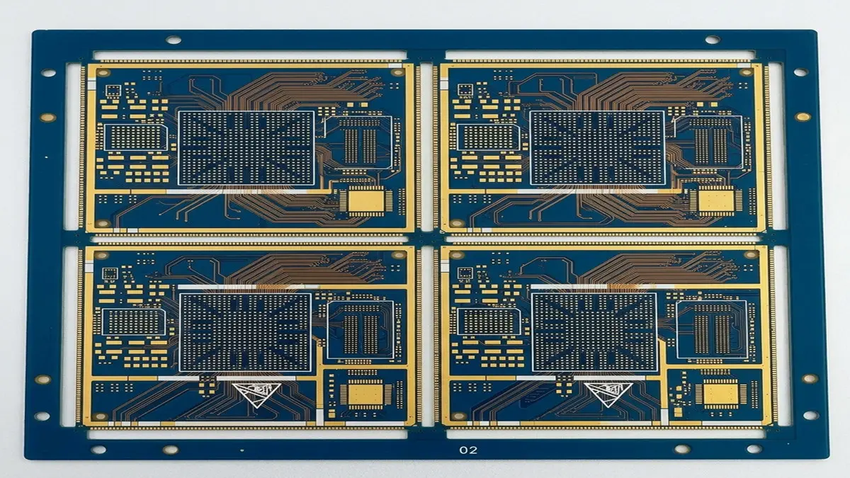
PCB Phototool Film Deformation and Annular Ring Misalignment Analysis
Negative‑film distortion rarely stems purely from poor‑quality raw film stock. Most real‑world defects come from cumulative physical stress: polyester base expansion and contraction from moisture gain/loss, heat generated inside exposure equipment, mechanical tension during plotting and handling, natural shelf‑age drift, plus uncontrolled workshop environmental swings. It is critical to distinguish stretch versus shrink effects: stretching pulls features outward, while shrinkage compresses feature dimensions inward, each demanding separate troubleshooting paths.
Process teams often confuse phototool film deformation with dry‑film lamination defects. These two failure modes produce visually similar misalignment yet carry different root causes and correction workflows. Film‑driven issues show corner‑to‑corner registration shift and annular‑ring eccentricity across the whole panel; dry‑film sticking problems manifest as local feature distortion limited to lamination zones. Use sequential process tracing: audit original artwork data, photoplot output, film storage conditions, all the way through pre‑exposure handling to isolate where dimensional drift originates. Real‑world US‑fabricator case patterns include corner registration offset, hole‑ring eccentricity, and inconsistent scaling between production batches. Understanding these root‑cause distinctions helps your procurement team avoid over‑paying for premium film when operational fixes deliver most of the improvement.
Temperature, Humidity, and Seasonal Compensation in U.S. PCB Shops
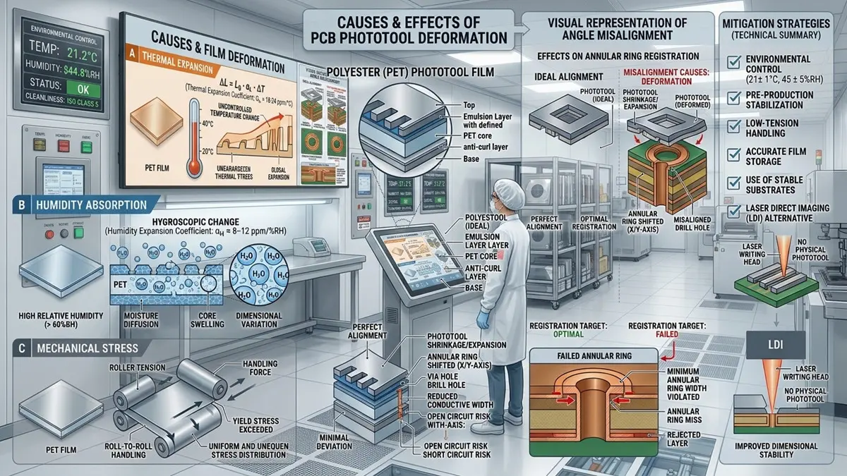
ISO Class 5 Cleanroom for PCB Phototool Storage and Laser Direct Imaging
Generic advice to “run constant temperature‑humidity” delivers little practical value without region‑specific tuning for North American manufacturing sites. Gulf‑coast and humid Mid‑western US PCB plants struggle with summer high‑humidity spikes, requiring dedicated dehumidification and film‑acclimatization buffer rooms. South‑west dry‑climate facilities face the opposite risk: excessive low relative humidity creates static discharge and film base shrinkage.
Your facility must define formal acclimatization dwell‑time for new film stock entering production floors, and prohibit frequent HVAC set‑point changes that trigger rapid environmental fluctuation. Apply thermal‑expansion coefficient calculations with both imperial (mil/inch) and metric (°C) units for cross‑team alignment. Build and maintain a living seasonal compensation table, updated monthly and per production batch, to offset predictable hot‑summer or dry‑winter dimensional shifts. Many competing technical resources skip these actionable operational details; correct seasonal compensation reduces unplanned rework far more effectively than simply upgrading film SKUs, which is a key consideration during procurement budget planning.
Film Storage, Incoming Inspection, and Shelf‑Life Drift
Even premium‑grade phototool film will deform if stored or mishandled post‑delivery. This section covers receiving, storage, and handling protocols complementary to environmental controls. Always retain original factory packaging, store film in total darkness, lay stock flat or hang vertically without heavy stacking pressure, and only touch film sheet edges during handling. Follow strict first‑in‑first‑out inventory rotation to limit natural dimensional drift from material aging.
Shelf‑life expiry dates are not your sole acceptance criterion: past storage history (transport temperature swings, warehouse exposure) can ruin film long before printed expiration dates. Implement a standardized incoming receiving checklist covering visual inspection, baseline dimensional measurement, reference hole‑position verification, and batch sample retention for traceability. US production facilities should label every film lot, maintain continuous environmental logs inside storage zones, and quarantine suspect stock. Train receiving and procurement staff to spot curled or warped incoming phototool sheets before they enter plotting workflows. Early rejection of compromised incoming material prevents costly downstream production scrap.
Measuring Deformation, Scaling Artwork, and Fixing Registration
Effective deformation correction requires a closed‑loop measurement‑to‑compensation workflow. First define key measurement targets: polyester base dimensional change, reference hole‑to‑hole pitch offset, and drift after repeated exposure cycles. Use certified reference steel rulers, optical metrology tools, and built‑in exposure‑registration targets, plus mandatory first‑article validation before full‑batch release.
Follow this repeatable sequence: lock fixed measurement benchmarks, calculate scaling‑offset ratios, generate compensated artwork, run small‑lot qualification, and sign‑off first‑article samples. Procurement and engineering teams must understand the risks of over‑compensation and endless iterative artwork revision, which can amplify errors rather than solving misalignment. A documented US‑shop case example illustrates high‑humidity summer‑week film expansion of several thousandths of an inch; engineers resolved registration errors using zone‑based scaling adjustments paired with fine‑tuned exposure‑chamber parameters. Procurement teams should evaluate metrology‑tool investments alongside film purchasing, as accurate measurement maximizes return from your phototool‑material spend.
Prevention SOPs, Stable Film Selection, and Exposure Hardware Choices
Long‑term deformation control combines standardized audit‑ready SOPs, smart film procurement, and strategic hardware investment. Build unified operational checklists covering incoming receiving, storage, environmental monitoring, exposure‑chamber maintenance, registration validation, and end‑of‑life film scrap criteria.
When sourcing phototool negatives, compare dimensional‑stability specifications of polyester base materials. Evaluate the trade‑offs between glass phototool plates versus conventional silver‑halide film negatives. Assess how vacuum hold‑down performance and contact‑exposure hardware influence apparent film distortion. Critically, define clear decision triggers for migrating toward laser direct imaging (LDI), rather than adopting blanket “replace‑all‑film” capital recommendations.
For US small‑to‑mid‑size PCB manufacturers, base your hardware‑upgrade business case on three measurable inputs: product precision requirements, production batch volume, and total cost of defects from mis‑registered panels. This framework helps procurement justify capital expenditure, balancing ongoing phototool‑film purchasing costs versus one‑time imaging‑equipment investment.
Next Steps & Downloadable Resource
Stop reacting to random registration failures. Download our free printable Phototool Negative‑Film Deformation Troubleshooting Checklist + Temperature‑Humidity Log Sheet. Run a 30‑day facility baseline measurement study across your plotting, storage, and exposure zones. Quantify your current rework yield loss caused by film‑related misalignment. Our technical specialists can support your team with phototool‑film specification reviews, supplier comparison assessments, and imaging‑hardware ROI evaluation. Reach out to turn measurement data into tangible improvements: lower scrap rates, higher registration yields, and predictable production throughput.
Frequently Asked Questions
What causes PCB negative film to stretch or shrink during the imaging process? Polyester‑base moisture absorption, exposure‑unit heat, mechanical tension, aging, and unstable ambient conditions combine to create stretch or shrinkage during plotting and contact exposure.
How do temperature, humidity, and seasonal swings affect phototool film stability? Relative‑humidity variation drives most polyester‑film dimensional change; seasonal weather shifts create predictable scaling drift requiring site‑specific compensation tables for US PCB workshops.
How can I measure film deformation and calculate the right artwork scaling compensation? Measure reference hole‑pitch and base‑film dimensions with calibrated metrology tools; compute scaling ratios, validate with small‑batch first‑article builds, and avoid excessive iterative compensation adjustments.
How do I correct registration misalignment caused by a deformed film negative? Start with root‑cause identification: separate film‑base distortion from dry‑film or equipment error. Apply artwork scaling compensation, improve acclimatization workflows, or retire severely deformed phototool sheets.
What storage, handling, and incoming inspection practices prevent negative‑film deformation? Use FIFO inventory rotation, low‑stress flat/hanging storage, full incoming‑lot dimensional checks, dark controlled‑humidity storage, and only handle sheets along edges.
What PCB failure modes can negative‑film deformation contribute to? Annular‑ring offset, poor hole‑registration, short/open circuits, inconsistent line‑width, cross‑batch yield variation, and higher scrap and rework expense.
When should a PCB shop switch from film phototools to laser direct imaging? Evaluate when high‑precision requirements, high scrap cost from film‑deformation defects, and production volume make LDI capital expenditure financially justified versus continuing phototool‑film procurement.
About Author
David Chen LinkedIn Profile
David Chen is a Senior RF/PCB Process Engineer at Shenzhen Hongda Circuit Technology Co., Ltd., with over 12 years of experience in high-frequency PCB fabrication, impedance-controlled stack-up design, and Rogers/PTFE laminate processing. He also boasts an extensive professional background in PCBA manufacturing, PCBA testing, and PCBA optimization, with specialized expertise in high-precision PCBA fault analysis and rigorous PCBA reliability testing. The author has worked with high-layer-count server PCB fabrication, ultra-low-loss backplane stackups, and thermo-mechanical reliability optimization for AI infrastructure projects involving 112G and 224G PAM4 architectures. Skilled in complex circuit design and cutting-edge advanced PCB manufacturing processes, he delivers solutions that elevate product durability and performance across industrial applications. His technical articles focusing on PCBA manufacturing workflows and testing methodologies are widely cited by industry peers and technical platforms, and have gained attention and recognition from industry colleagues.