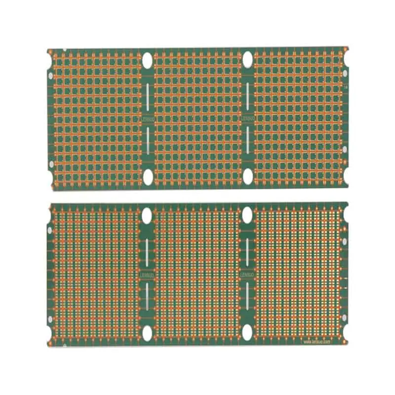
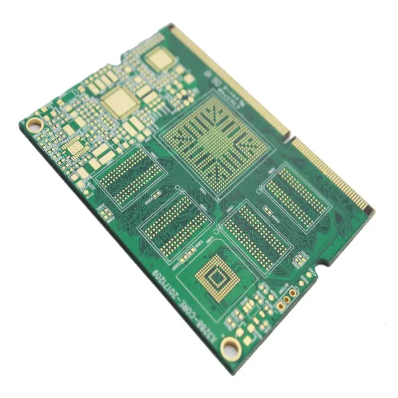
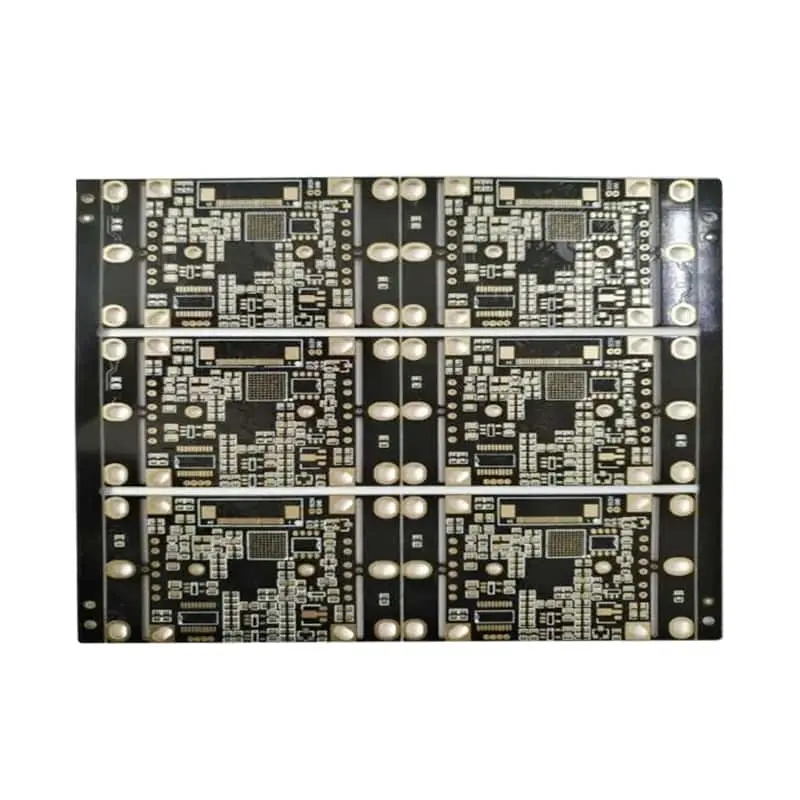
Driver Circuit Board: Design, PCB Manufacturing, Assembly, and Supplier Selection
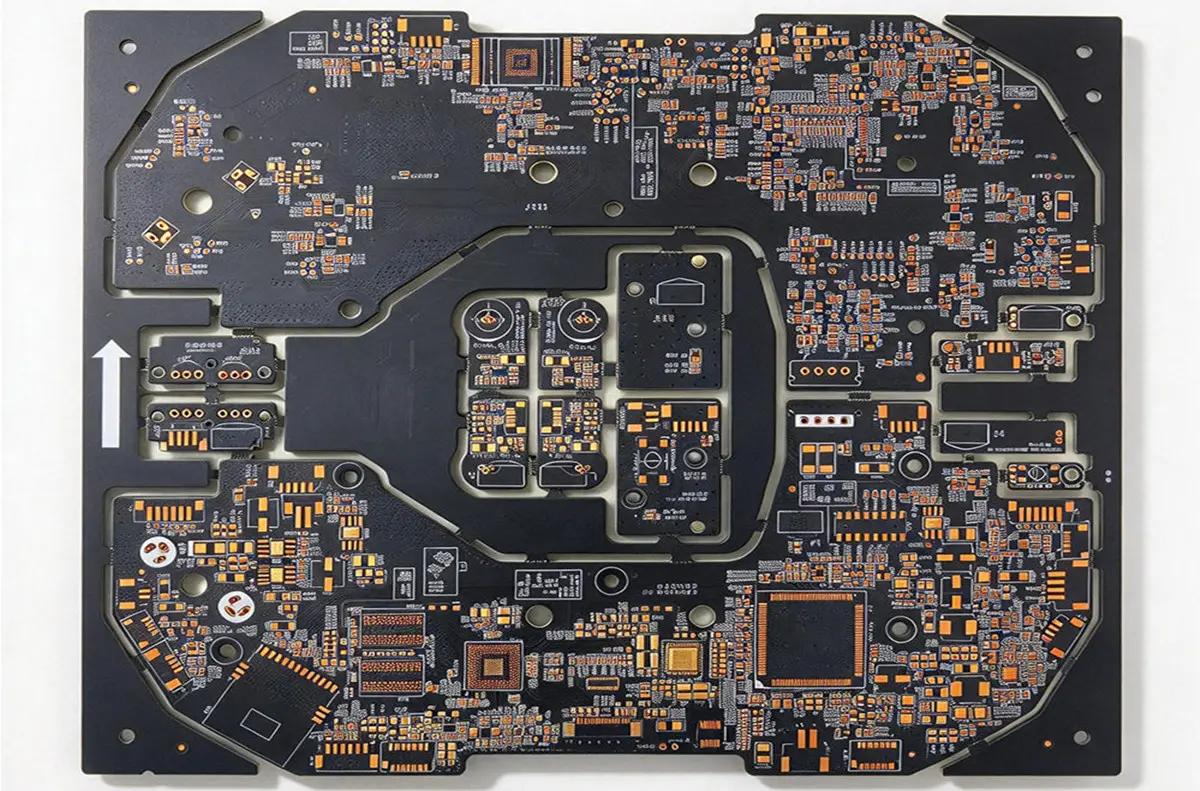
A driver circuit board converts control signals into the electrical power needed to operate LEDs, motors, power switches, and other electronic loads. For OEMs and industrial equipment manufacturers, selecting the right driver circuit board requires more than matching voltage and current ratings. PCB layout, component selection, thermal performance, electromagnetic interference (EMI), protection circuits, and manufacturing quality all affect product reliability.
HAODA ELECTRONIC CO.,LIMITED. supports PCB manufacturing and PCBA assembly for electronic products requiring application-specific circuit board solutions. Whether you are developing a prototype, optimizing an existing design, or preparing for volume production, understanding these engineering and sourcing requirements helps reduce development risks and improve manufacturing readiness.
What Are the Main Types of Driver Circuit Boards and Their Applications?
 https://www.pcbcoming.com/product/
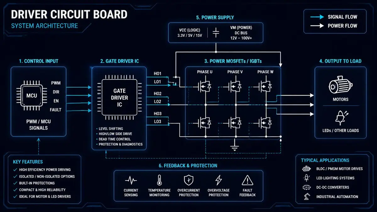
Driver Circuit Board System Architecture & Signal Flow Diagram
A driver circuit board regulates or switches electrical power according to a control signal. Its architecture depends on the load, operating voltage, current requirements, switching frequency, and protection needs.
| Driver circuit board type | Main components | Typical applications | Key selection criteria |
|---|---|---|---|
| Constant-current LED driver | Driver IC, switching MOSFET, inductor, current-sense resistor | LED lighting, indicators, industrial illumination | Current accuracy, efficiency, dimming range, thermal performance |
| MOSFET/IGBT gate driver | Gate-driver IC, gate resistor, protection circuitry | Inverters, power converters, industrial switching systems | Gate voltage, peak drive current, switching speed, isolation |
| H-bridge motor driver | Four switching devices or an integrated bridge, current sensing, control logic | Robotics, actuators, small electric drives | Motor stall current, voltage drop, reverse-current handling |
| Isolated gate-driver board | Isolated driver, isolation barrier, isolated power supply | High-voltage converters, industrial power electronics | Isolation rating, common-mode transient immunity, creepage |
| Low-voltage switching power driver | Controller IC, MOSFETs, inductors, capacitors | Embedded systems, battery-powered electronics | Input range, output regulation, efficiency, transient response |
The typical signal and power paths are:
- LED driver: DC input → switching converter → current regulation → LED load.
- Motor driver: PWM/control input → gate driver or bridge controller → power switches → motor.
- Gate-driver board: PWM command → isolation or level shifting → gate driver → MOSFET/IGBT gate.
- Switching power driver: DC input → switching stage → filtering and feedback → regulated output.
For a 12 V automotive accessory, designers must consider supply transients and reverse-polarity protection. A 24 V industrial controller may require stronger noise immunity and protection against inductive loads. LED lighting emphasizes current regulation and thermal management, while robot and drone motor drivers must accommodate startup and stall currents.
The correct choice depends on the complete electrical operating envelope, not simply the nominal voltage.
How Do You Choose a Driver Circuit Board Using Datasheet Specifications?
Before requesting a quotation, define the operating voltage, continuous and peak current, switching frequency, load characteristics, ambient temperature, and required protection functions. Then verify that the selected components can withstand actual operating conditions.
| Parameter | What it means | What buyers should verify |
|---|---|---|
| Drain-source voltage (VDS) | Maximum rated voltage across a MOSFET | Adequate margin for input variation and switching transients |
| Continuous and pulsed current | Current limits under specified conditions | Package, PCB copper, cooling, pulse duration, and duty cycle |
| RDS(on) | MOSFET on-state resistance | Resistance at the actual gate voltage and operating temperature |
| Gate charge (Qg) | Charge required to switch the gate | Driver current capability and switching losses |
| Turn-on/off time | Switching transition characteristics | Switching frequency, losses, and EMI |
| Safe operating area (SOA) | Permitted voltage-current operating combinations | Startup, fault, and transient conditions |
| Thermal resistance (θJA/θJC) | Relationship between power dissipation and temperature rise | Actual board layout, heatsinking, and cooling conditions |
| Protection thresholds | Overcurrent, undervoltage, or overtemperature limits | Compatibility with the load and fault response |
Example: estimating MOSFET conduction loss
Assume a MOSFET carries 10 A continuously and has an RDS(on) of 10 mΩ at the relevant operating conditions.
Pconduction = I² × RDS(on)
Pconduction = 10² × 0.010 = 1 W
This 1 W estimate excludes switching, gate-drive, and other losses. If switching loss adds another 0.5 W, the estimated total for that MOSFET becomes 1.5 W before accounting for additional losses.
If the allowable junction temperature is 125°C and the design target is 100°C at a 40°C ambient temperature, the available temperature rise is 60°C. A simplified thermal budget gives:
θJA, effective ≤ 60°C / 1.5 W = 40°C/W
This is a preliminary screening calculation, not proof that the device will remain within its limits. The actual thermal path, transient behavior, enclosure, and neighboring heat sources must be evaluated.
When comparing components, review manufacturer datasheets rather than comparing headline current ratings alone. For example, the Infineon IRLZ44N and Texas Instruments CSD18540Q5B represent different MOSFET design options, but neither should be selected without checking voltage rating, gate-drive requirements, package thermal characteristics, availability, and suitability for the application. Verify current datasheets and lifecycle status before purchasing.
How Do You Interface a Driver Circuit Board With Arduino, ESP32, or STM32?
A microcontroller typically supplies logic signals, while a driver stage handles the voltage and current needed by the load. The interface must match logic thresholds, signal polarity, timing, and isolation requirements.
A typical connection is:
Microcontroller PWM output → driver input → gate driver or bridge → power switches → load
Connect the controller and driver grounds as specified by the circuit architecture. Isolated designs may require separate ground domains and an appropriate isolated power supply. Never assume that a 3.3 V GPIO can directly drive a MOSFET gate adequately; logic compatibility and gate-drive performance are separate requirements.
For half-bridge or full-bridge designs, complementary switching signals must include sufficient dead time to prevent simultaneous conduction of the high-side and low-side switches. The required dead time depends on device switching characteristics, driver propagation delays, and operating conditions.
A simplified firmware sequence is:
// Conceptual pseudocode; adapt to the target MCU and driver.
initialize_pwm();
disable_power_stage();

set_pwm_frequency(target_frequency);
set_dead_time(validated_dead_time);

enable_fault_monitoring();

for (int duty = 0; duty <= startup_limit; duty++) {
    if (fault_detected()) {
        disable_power_stage();
        report_fault();
        break;
    }

    set_pwm_duty(duty);
    wait_for_control_interval();
}
The function names are illustrative, not a ready-to-compile library. Use the microcontroller’s hardware PWM or complementary PWM peripherals where available, and implement hardware interlocks and fault shutdown independently of normal firmware execution.
PWM frequency also affects switching losses, acoustic behavior, and EMI. Higher frequency may reduce passive-component size but increase switching losses. Validate the frequency, resolution, and dead time on the actual hardware before connecting the final load.
How Should Driver Circuit Board PCB Layout, Thermal Management, and EMI Protection Be Designed?
A driver circuit board can fail even when every component meets its individual datasheet specifications. High-current loops, poor return paths, insufficient copper, and excessive switching-node coupling can create overheating, oscillation, or electromagnetic interference.
Use these PCB layout priorities during design and manufacturing review:
- Minimize high-current loops. Place switching devices, local decoupling capacitors, and freewheel paths close together to reduce parasitic inductance.
- Separate sensitive signals from switching nodes. Keep gate-drive and current-sense routing away from noisy power paths.
- Plan the return-current path. Use a deliberate ground strategy, with separation between power and sensitive control regions where appropriate. Avoid indiscriminate ground-plane splits that interrupt return paths.
- Select copper weight and trace width together. Estimate current capacity and temperature rise using an appropriate PCB trace model, then validate with thermal testing. Internal layers, ambient temperature, and airflow can change the result.
- Design for heat removal. Use copper planes, suitable thermal vias, and adequate component spacing where the stackup and assembly process support them.
- Control switching transients. Evaluate gate resistors, snubbers, TVS devices, and local filtering based on measured waveforms rather than adding components without diagnosis.
For thermal evaluation, estimate conduction loss and switching loss separately, then calculate junction temperature using the applicable thermal model. Copper area alone does not determine performance; board thickness, via construction, component package, airflow, and enclosure all matter.
EMI mitigation should begin with layout and switching-loop control. Additional measures may include input filtering, common-mode chokes, differential capacitors, RC snubbers, and appropriate shielding or grounding. Each modification should be checked for effects on stability, efficiency, and component stress.
For products sold in the United States, determine applicable FCC requirements for unintentional radiators and any relevant UL or IEC safety standards based on the product category. High-voltage designs also require suitable creepage, clearance, insulation, and dielectric withstand considerations. Compliance depends on the complete product and intended use, not the PCB alone.
During supplier evaluation, confirm that the PCB manufacturer can meet the required layer count, copper weight, minimum trace and spacing, hole specifications, material requirements, and fabrication tolerances. For PCBA, review component sourcing, soldering process control, inspection, and test requirements before production release.
How Do You Test a Driver Circuit Board and Decide Whether to Buy or Build It?
Validate a new driver board in stages, beginning with unpowered inspection and progressing to controlled electrical and thermal testing.
Pre-power checklist
- Confirm component orientation, polarity, solder joints, and connector pinout.
- Check supply-to-ground resistance and investigate unexpected shorts.
- Verify power-device ratings and gate-drive voltage limits.
- Confirm current-sense connections and protection thresholds.
- Use a current-limited supply for initial energization.
Powered validation
- Check supply rails and controller logic levels before enabling the power stage.
- Observe PWM, gate-source voltage, and switching-node waveforms with appropriately rated probes.
- Measure input current, load current, and voltage drop under controlled load conditions.
- Check for ringing, overshoot, shoot-through, and unexpected oscillation.
- Use a thermal camera or temperature sensors to evaluate component and PCB temperatures at increasing loads.
- Test current limiting, thermal shutdown, undervoltage response, and fault recovery where applicable.
Common failure symptoms include excessive MOSFET heating, gate-voltage overshoot, intermittent operation, solder-joint cracking, and overcurrent trips. Diagnose the waveform and thermal behavior before changing components. High-voltage switching measurements should be performed by qualified personnel using appropriately rated equipment and safe procedures.
Should you build or buy a driver circuit board?
| Consideration | In-house design | Outsourced PCB/PCBA or commercial module |
|---|---|---|
| Initial engineering cost | Higher when design and validation start from scratch | Can reduce internal fabrication and assembly workload |
| Customization | Maximum control over architecture | Depends on design ownership and supplier capability |
| Time to market | Depends on design and debugging cycles | May shorten production preparation when documentation is complete |
| Quality responsibility | Primarily internal | Shared through defined specifications, acceptance criteria, and supplier controls |
| Certification | Requires internal planning and testing | Supplier support may help, but product-level compliance remains the buyer’s responsibility |
For a small prototype run, a commercial module may be the fastest route if its ratings and interfaces meet the requirements. For a proprietary product or volume program, custom PCB manufacturing and PCBA assembly may provide better control over footprint, thermal design, sourcing, and integration.
Build a total-cost estimate that includes engineering time, PCB fabrication, components, assembly, test fixtures, rework, certification, and production yield. Obtain current component quotations from authorized distributors such as DigiKey and Mouser, and compare assembly quotations against the same BOM and test scope.
How Can You Request a Driver Circuit Board Manufacturing and Assembly Quote?
HAODA ELECTRONIC CO.,LIMITED. provides PCB manufacturing and PCBA assembly support for OEMs developing electronic products. To evaluate a driver circuit board project, prepare the following information:
- Gerber or ODB++ fabrication files and the PCB stackup, if available.
- BOM with manufacturer part numbers and approved alternatives.
- Assembly drawings, pick-and-place files, and special process requirements.
- Operating voltage, continuous and peak current, switching frequency, and thermal limits.
- Required inspection, electrical testing, traceability, and production quantities.
For early-stage projects, include a schematic and functional description so that manufacturing questions can be identified before the first build. Engineering design validation and power-electronics safety certification should be agreed upon separately from standard PCB fabrication and assembly.
Request a Driver Circuit Board PCB/PCBA Quote
Contact HAODA ELECTRONIC CO.,LIMITED. to discuss prototype builds, small-batch production, or volume manufacturing.
- Website: https://www.pcbcoming.com/
- Email: pcb@pcbcoming.com
Submit your design files, target quantity, and delivery requirements to request a project review and quotation. Include your testing and compliance expectations so the manufacturing scope can be evaluated accurately.
Frequently Asked Questions About Driver Circuit Boards
What are the main types of driver circuit boards, and which should I use for LEDs, motors, or gates?
Use a constant-current driver for LEDs, a suitable H-bridge or motor-control stage for reversible motors, and a MOSFET/IGBT gate-driver circuit for power-switch control. Confirm voltage, current, switching, protection, and thermal requirements before selection.
How do I read a MOSFET or IGBT datasheet to determine voltage, current, and thermal limits?
Review the voltage rating, current conditions, SOA, switching characteristics, gate-drive requirements, and thermal data. Apply derating and evaluate actual operating conditions rather than relying solely on the headline current rating.
What PCB layout rules matter most for high-current driver boards?
Minimize high-current loops, provide controlled return paths, separate sensitive signals from switching nodes, size copper for the thermal load, and use thermal vias where appropriate. Verify the design through electrical and temperature testing.
How do I safely connect an Arduino, ESP32, or STM32 to a driver board?
Check logic-level compatibility, input thresholds, grounding, gate-driver requirements, and isolation. Use suitable PWM hardware, validated dead time for bridge circuits, soft-start logic, and independent hardware fault protection.
Which tests should I perform before connecting the final load?
Start with visual inspection and unpowered checks. Then use current-limited power, verify supply rails and switching waveforms, measure current, check thermal performance, and validate protection functions under controlled conditions.
Should I buy a commercial driver board or manufacture a custom PCB?
Buy a commercial board when its ratings, interfaces, documentation, and reliability meet your needs. Consider a custom PCB/PCBA when product integration, form factor, component selection, production control, or long-term supply requirements justify the additional engineering and validation effort.
About Author
David Chen LinkedIn Profile
David Chen is a Senior RF/PCB Process Engineer at Shenzhen Hongda Circuit Technology Co., Ltd., with over 12 years of experience in high-frequency PCB fabrication, impedance-controlled stack-up design, and Rogers/PTFE laminate processing. He also boasts an extensive professional background in PCBA manufacturing, PCBA testing, and PCBA optimization, with specialized expertise in high-precision PCBA fault analysis and rigorous PCBA reliability testing. The author has worked with high-layer-count server PCB fabrication, ultra-low-loss backplane stackups, and thermo-mechanical reliability optimization for AI infrastructure projects involving 112G and 224G PAM4 architectures. Skilled in complex circuit design and cutting-edge advanced PCB manufacturing processes, he delivers solutions that elevate product durability and performance across industrial applications. His technical articles focusing on PCBA manufacturing workflows and testing methodologies are widely cited by industry peers and technical platforms, and have gained attention and recognition from industry colleagues.