A PCB via current calculator is an engineering tool that estimates how much electrical current a plated through-hole, blind via, or buried via can safely carry before its temperature rise exceeds a specified limit. For procurement teams, design engineers, and hardware program managers sourcing boards in the North American supply chain, this tool answers one deceptively simple question early in the design cycle: how many vias do I need, and how big do they need to be?
This article explains what the tool does, what it doesn’t do, the inputs it requires, the math behind it, a worked example you can verify yourself, and the standards and testing practices that turn an estimate into a manufacturable, reliable design.
What a PCB Via Current Calculator Is and Why Engineers Use It
A via current calculator estimates the current-carrying capacity of a plated hole at a given allowable temperature rise — typically +10 °C or +20 °C above ambient. It is used at the schematic and pre-layout stage to:
Size via chains in switch-mode power supplies (e.g., from input rail to MOSFET drain)
Plan thermal via arrays under hot components (DC-DC converters, motor drivers, RF power amplifiers)
Verify BGA power/ground return paths and decoupling capacitor via connections
Assign trace and copper weights before committing to a stackup with your fab house
The critical distinction many online tools omit: a calculator is a screening tool, not a certification tool. Use it for first-pass layout decisions, prototype planning, and cost estimation. You must move to finite-element thermal simulation or vendor-validated data when any of the following apply:
Decision rule: if the calculated temperature rise is marginal (within 20% of your limit), or the current exceeds ~5 A per via, escalate to thermal simulation or request a sample-board loading test from your fabricator before freezing the layout.
Key Inputs and Manufacturing Factors That Affect Via Current Capacity
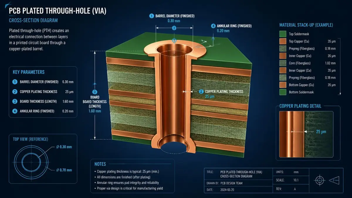
Key Inputs and Manufacturing Factors Affecting PCB Via Current Capacity
Accurate results require six physical inputs — and nearly all of them must be confirmed with your PCB manufacturer before you trust the output:
Drill diameter (barrel ID) — e.g., 12 mil (0.30 mm) finished hole
Plating thickness — e.g., 25 µm (~1 mil), 50 µm (2 mil), or thick-copper plating; note that “1 oz copper” on outer layers (~35 µm) does not automatically mean the via barrel received 1 oz of plating
Board thickness / via length (L) — e.g., 1.6 mm (63 mil) or a 100 µm microvia depth
Parallel via count and spacing — vias share current only if symmetrically connected at both ends
Allowable temperature rise (ΔT) — +10 °C for conservative designs, +20 °C common for cost-driven consumer work
Thermal environment — inner-layer via thermally coupled to a plane behaves very differently from an outer-layer via in still air
Manufacturing and cost trade-offs buyers must understand:
Unfilled vs. filled vias: Open vias are cheapest; filled-and-capped vias (for via-in-pad) cost 20–40% more per hole but eliminate acid-trap reliability risk and improve heat spreading into thermal pads.
Plating thickness: Standard plating is 20–25 µm. Asking for 2–3 oz-equivalent barrel plating adds process steps and cost, and many shops cap barrel plating at ~50 µm for aspect ratios above 8:1.
Aspect ratio limits: A 1.6 mm board with a 0.2 mm drill is 8:1 — near the reliability ceiling for many US shops. Thicker plating demands larger drills or thinner cores.
Microvias/blind vias: Feasible but sequential lamination raises cost 30–60%; microvia current capacity is typically under 1 A each and they are almost always used in clusters.
Action item: before running calculations, email your fabricator and confirm drill diameter, minimum plating thickness guarantee (not nominal), aspect ratio capability, and fill/cap options for your stackup.
Underlying Calculation Methods and Key Formulas
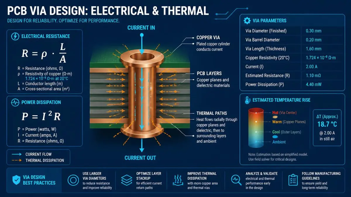
Underlying Calculation Methods and Key Formulas for PCB Via Current
Every credible via current calculator reduces to three equations.
Step 1 — Barrel resistance (accounting for temperature):
R=Aρ⋅L
where the hollow-cylinder cross-section is:
A=π⋅(router2−rinner2)=π⋅tplating⋅(dinner+tplating)
Copper resistivity at temperature T:
ρ(T)=ρ20⋅[1+α⋅(T−20°C)],ρ20=1.72×10⁻⁸Ω⋅m,α≈0.0039/°C
Step 2 — Power dissipation: P=I2R . Self-heating raises ρ, which raises R — for small ΔT this is usually ignored, but at ΔT > 30 °C the positive feedback matters (roughly +8% resistance per 20 °C).
Step 3 — Temperature rise: the standard simplification models the via as a small heat source dissipating into the board:
ΔT=I2R⋅Rth
where thermal resistance Rth is taken from IPC-2152 empirical charts (roughly 80–150 °C/W for a 12–13 mil via in 1.6 mm FR-4, falling substantially when the via lands on a solid plane). More rigorous tools replace the single Rth with a thermal resistance network: barrel → pad → plane → board surface → air.
Parallel vias: N identical, symmetrically connected vias reduce resistance and heating by ~1/N (slightly better in practice because adjacent vias share board heat-sinking). Never assume current sharing among vias with unequal path lengths — asymmetry can concentrate 2× the average current in the lowest-resistance via.
What most web calculators get wrong: omitting ρ₀ = 1.72×10⁻⁸ Ω·m, quoting thermal resistance without stating the board/plane assumption, and ignoring skin depth (δ ≈ 66/√f µm in copper — at 100 kHz, current already crowds to the outer ~0.2 µm of the barrel surface, changing effective resistance and current crowding entirely).
Worked Example and Typical Current Capacity Ranges
Example: finished drill 0.30 mm (12 mil), plating 25 µm, board 1.6 mm, ΔT limit +10 °C, 25 °C ambient, via connects to a ground plane.
Step 1 — Cross-section: A = π · 0.000025 m · (0.00030 + 0.000025) m = 2.55 × 10⁻⁸ m²
Step 2 — Resistance at 20 °C: R = (1.72 × 10⁻⁸ × 0.0016) / 2.55 × 10⁻⁸ ≈ 1.08 mΩ (≈ 1.17 mΩ at 30 °C)
Step 3 — Heating: with IPC-2152 empirical thermal resistance ≈ 90 °C/W for a plane-connected via: ΔT = I² · 0.00108 · 90 = 0.097 · I²
Setting ΔT = 10 °C: I ≈ 10 A. One via is marginal at 10 A; at 5 A, ΔT ≈ 2.4 °C — comfortable.
Parallel sharing check: two vias → ~0.5 mΩ equivalent, ΔT at 10 A drops to ~2.5 °C. Four vias → ~0.27 mΩ, ΔT < 1 °C.
Typical continuous-current capacity (empirical, 1.6 mm FR-4, +10 °C rise, plane-connected)
| 0.20 mm (8 mil) | 20 µm | 2.5–3 A | 1.0 A per 0.1 mm drilled, 1 oz plating |
| 0.30 mm (12 mil) | 25 µm | 8–12 A | ~10 A at 25 µm |
| 0.40 mm (16 mil) | 35 µm | 15–20 A | +40% vs. 12 mil |
| Microvia 0.10 mm | 15–20 µm | 0.5–1 A | Always use clusters |
| 0.30 mm | 50 µm (2 oz) | 18–22 A | Thick plating nearly doubles capacity |
Reliability rule: if your calculated result leaves <50% thermal margin, reduce target current per via or add parallel vias. Thermal cycling fatigue accumulates fastest when vias run near their rated ΔT.
Standards, Safety Margins, Testing, and Reliability Considerations
Standards to reference:
IPC-2152 — the current authoritative standard for conductor current-temperature charts, including via charts (supersedes IPC-2221 Appendix charts for via work)
IPC-2221 — general design standard; still widely cited for legacy internal copper and board density rules
UL/IEC product safety practice — for mains-connected or certified products, documented thermal margins are expected in the technical file
Derating guidance: apply an environmental multiplier (sealed enclosures: use 70–80% of free-air capacity), cap ΔT at +10 °C for long-life or high-cycle products, and +20 °C only for cost-driven designs with ample via count. For thermal-cycling endurance, keep operating ΔT ≤ 50% of the tested rating.
Lab verification methods (what to ask your lab or fab partner for):
Four-terminal resistance measurement of the via chain at 1 A DC — confirms plating integrity and gives true barrel resistance
Infrared thermography or 0.5 mm thermocouple bonded to the via pad — ramp current in 1 A steps, hold 5 min each, record ΔT vs. current curve
Sample loading test — run the populated board at worst-case load for 2+ hours; verify ΔT and check for resistance drift (indicates barrel micro-cracking)
Manufacturing cost interplay: requesting 50 µm plating on a high-aspect-ratio board may force a larger drill, changing the current capacity back down — iterate the calculator with guaranteed fab values, not nominal ones.
Checklist to send your fabricator: finished drill sizes, minimum plating guarantee (µm), aspect ratio capability, fill/cap options, thermal test data or qualification reports for their plating process.
Get Your Free Via Sizing Worksheet and DFM Review
Download our Excel via current calculator template — with one-click mil/mm/µm/oz unit conversion, parallel-via sharing, and the comparison table above built in — and use it in your next design review.
Send us your board thickness, target current, and stackup and our US-based applications engineers will return a free manufacturability assessment within one business day (US time zones), including recommended drill/plating combinations and a sample-board thermal test option. [Request your free DFM review →] [Download the calculator →]
FAQ
What input parameters do I need to use a PCB via current calculator accurately?
Finished drill diameter, plating thickness (guaranteed minimum from your fab), board thickness/via length, number of parallel vias, allowable temperature rise, ambient conditions, and whether the via thermally connects to a plane.
How do you calculate the electrical resistance of a plated via?
R = ρ·L/A, where A = π·t·(d + t) for a hollow barrel, ρ₂₀ = 1.72×10⁻⁸ Ω·m, and ρ increases ~0.39% per °C above 20 °C. See the worked example above.
How do plating thickness and barrel diameter affect current capacity?
Both increase the copper cross-section linearly, so capacity scales roughly with plating thickness × diameter. Doubling plating from 25 µm to 50 µm roughly doubles a via’s safe current at the same ΔT.
How many vias are needed in parallel for 5 A or 10 A?
For 5 A: one 12 mil/25 µm via is marginal — use two. For 10 A: use two to four 12 mil vias, or one 16 mil/35 µm via, depending on reliability requirements.
Which IPC standards should I reference?
IPC-2152 for current-temperature data (including vias); IPC-2221 for general design practice. For certified products, align with your NRTL’s thermal documentation expectations.
What lab tests verify via current capacity?
Four-terminal resistance measurement, IR thermography or thermocouple ΔT-vs-current sweeps on sample boards, and long-duration loading tests for cycling endurance.
When should I use finite-element thermal simulation instead?
When per-via current exceeds ~5 A, when vias sit on thick copper or unusual dielectrics, for high-frequency (skin-effect) currents, for microvia stacks, or whenever the calculator result is within 20% of your temperature-rise limit.
About Author
David Chen LinkedIn Profile
David Chen is a Senior RF/PCB Process Engineer at HAODA ELECTRONIC CO.,LIMITED., with over 12 years of experience in high-frequency PCB fabrication, impedance-controlled stack-up design, and Rogers/PTFE laminate processing. He also boasts an extensive professional background in PCBA manufacturing, PCBA testing, and PCBA optimization, with specialized expertise in high-precision PCBA fault analysis and rigorous PCBA reliability testing. The author has worked with high-layer-count server PCB fabrication, ultra-low-loss backplane stackups, and thermo-mechanical reliability optimization for AI infrastructure projects involving 112G and 224G PAM4 architectures. Skilled in complex circuit design and cutting-edge advanced PCB manufacturing processes, he delivers solutions that elevate product durability and performance across industrial applications. His technical articles focusing on PCBA manufacturing workflows and testing methodologies are widely cited by industry peers and technical platforms, and have gained attention and recognition from industry colleagues.