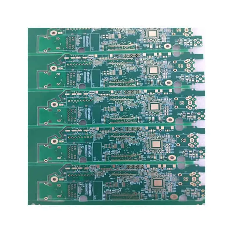
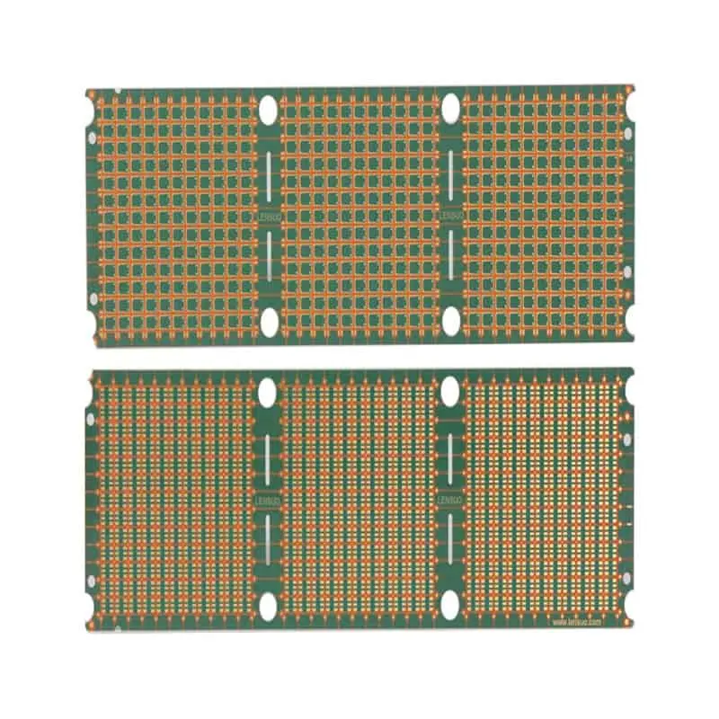
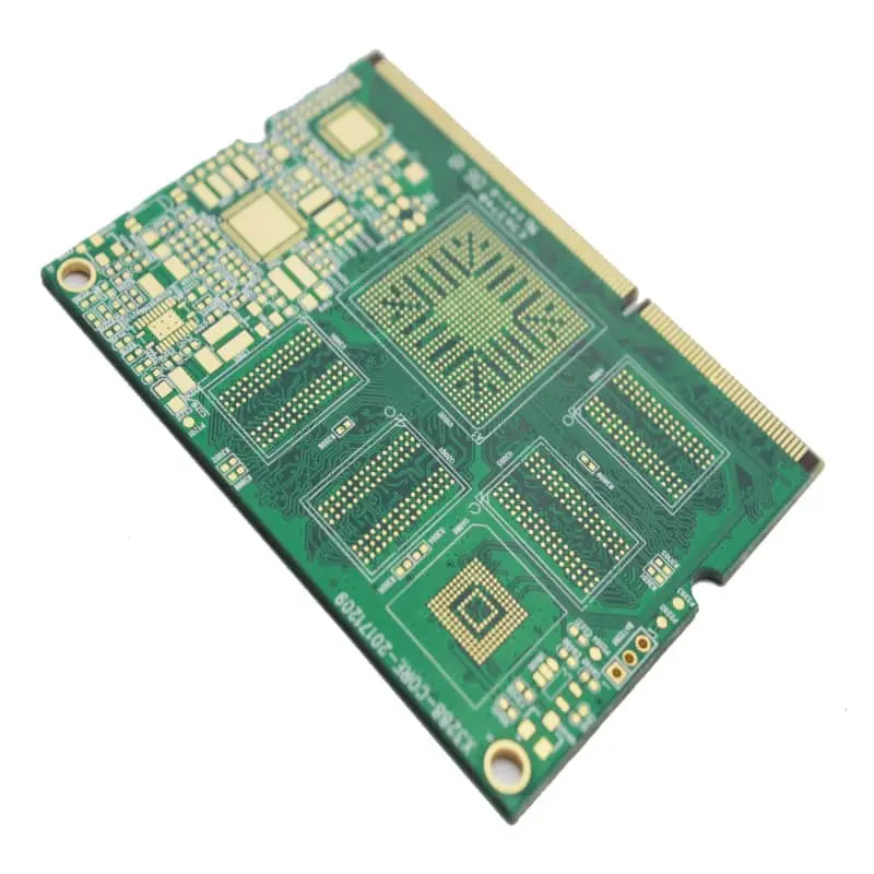
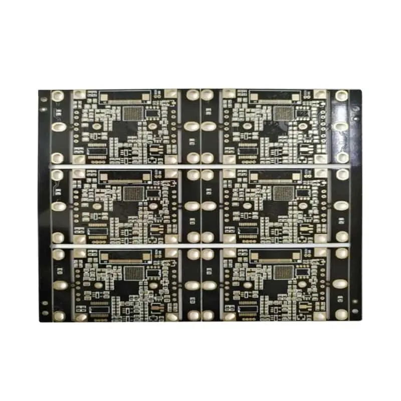
When a PCB carries high-speed signals, impedance control is not simply a routing preference—it is a manufacturing requirement. A reliable impedance controlled PCB requires a defined stackup, controlled dielectric thickness, trace geometry, copper structure, validated fabrication tolerances, and TDR verification against the customer’s target impedance.
For engineers and procurement teams, the key question is not only whether a PCB manufacturer claims “controlled impedance,” but whether it can translate your design target into a manufacturable stackup, hold the required tolerances, verify impedance with test coupons, and provide measurable production evidence.
What Is PCB Impedance and Why Does It Matter for Signal Integrity?
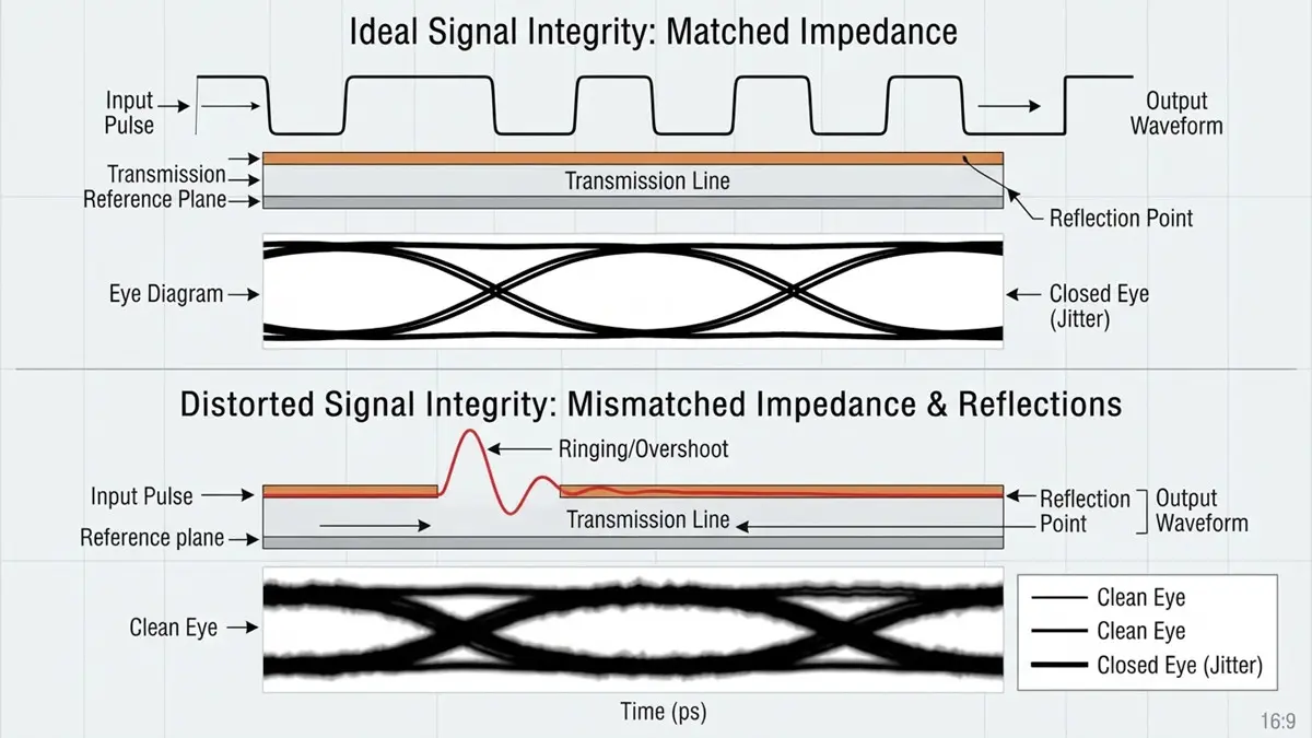
Impedance Controlled PCB Signal Integrity & Eye Diagram Analysis
PCB characteristic impedance is the electrical impedance experienced by a high-frequency signal traveling along a transmission line. It is primarily determined by conductor geometry, dielectric properties, distance to the reference plane, and the surrounding structure. When the PCB impedance does not match the intended system impedance, part of the signal can be reflected, increasing jitter, reducing eye opening, and potentially causing communication failures.
For a simplified transmission line:
Z₀ ≈ √(L/C)
where Z₀ is characteristic impedance, L is inductance per unit length, and C is capacitance per unit length.
Consider a 50 Ω single-ended transmission line connected to a 50 Ω receiver. The transition is approximately matched. If the PCB section instead presents a substantially different impedance, the reflection coefficient can be approximated by:
Γ = (ZL − Z₀) / (ZL + Z₀)
where ZL is the load impedance.
This becomes increasingly important as signal rise time decreases. A PCB trace can behave as a transmission line even when its nominal data rate is not extremely high because the electrical behavior is strongly related to edge rate and propagation delay.
USB, PCIe and Ethernet designs commonly use controlled-impedance interconnects. The actual target must come from the applicable interface specification and system design rather than from a generic PCB rule.
PCB construction also affects how easily impedance can be controlled:
| PCB Type | Impedance-Control Consideration |
|---|---|
| Single-sided PCB | Limited reference-plane control; generally unsuitable for demanding controlled-impedance structures |
| Double-sided PCB | Possible for selected structures, but geometry and reference-plane control are more constrained |
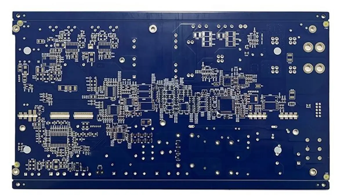
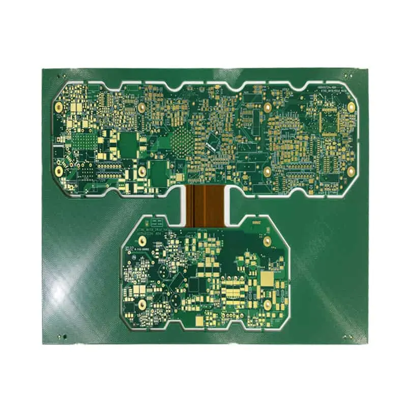
| Multilayer PCB | Provides dedicated reference planes and greater control of microstrip/stripline structures |
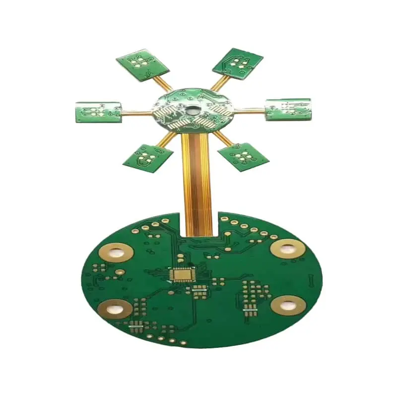
| HDI PCB | Enables dense high-speed routing but requires careful control of microvias, dielectric thickness and transitions |
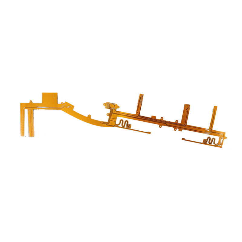
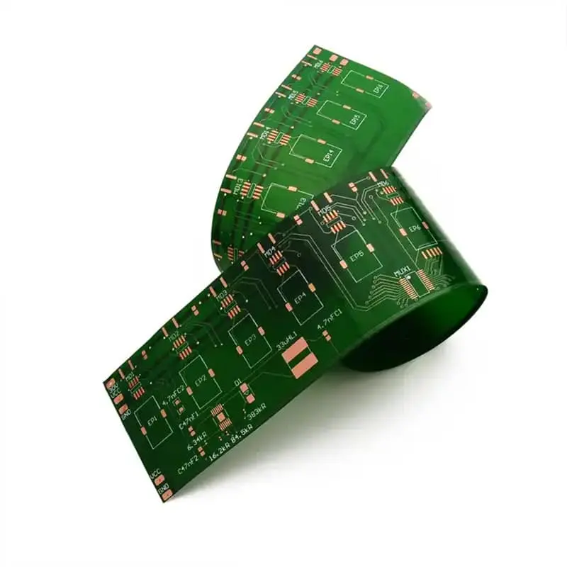
| Flexible PCB | Requires consideration of flexible dielectric and coverlay thickness in addition to conductor geometry |
For procurement, this means the PCB supplier should review the electrical requirement together with the physical stackup before quoting a controlled-impedance board.
How Do Stackup, Materials, and Trace Geometry Determine Target Impedance?
Target impedance is established by the interaction of dielectric thickness, dielectric constant, copper thickness, trace width, trace spacing, reference-plane geometry, and surface structures such as solder mask. A manufacturer should therefore calculate impedance from the proposed stackup rather than simply assigning a standard trace width.
For a microstrip, impedance is influenced strongly by the relationship between trace width W and dielectric height H. A simplified approximation often used for preliminary engineering is:
Z₀ ≈ (87 / √(εr + 1.41)) × ln(5.98H / (0.8W + T))
where εr is relative dielectric constant, H is dielectric height, W is trace width, and T is conductor thickness. This is a preliminary approximation—not a substitute for a field solver or fabricator stackup calculation.
For stripline structures, the conductor is surrounded by dielectric and referenced by planes on both sides. The resulting impedance depends on the conductor width, copper thickness, dielectric thickness above and below the trace, and dielectric constant.
Example engineering starting points
The following values are illustrative calculation targets, not universal manufacturing dimensions:
| Target | Structure | Typical Design Variables |
|---|---|---|
| 50 Ω | Single-ended microstrip | Trace width, dielectric height, copper thickness, εr |
| 50 Ω | Single-ended stripline | Trace width, copper thickness, dielectric spacing, εr |
| 90 Ω | Differential pair | Trace width, pair spacing, dielectric height, copper thickness, εr |
| 100 Ω | Differential pair | Trace width, pair spacing, dielectric height, copper thickness, εr |
A production manufacturer should calculate the final geometry using the actual material system and finished copper condition.
Material selection matters. Standard FR-4 can support many digital applications, but its effective dielectric behavior varies by resin content, glass style, frequency, and construction. High-frequency materials such as Rogers systems may be selected when dielectric loss, electrical stability, or RF performance becomes critical. Flexible circuits require additional consideration of the flexible dielectric and coverlay.
Solder mask can also change the effective electrical environment around an outer-layer microstrip. For tightly controlled high-speed designs, the manufacturer should know whether impedance is calculated with the intended solder-mask structure included or excluded.
Copper surface roughness is another manufacturing variable. At higher frequencies, conductor roughness increases effective RF loss and can influence transmission-line behavior. Similarly, final copper thickness after plating can differ from the nominal starting foil thickness. These parameters should therefore be incorporated into the manufacturer’s impedance calculation.
For RFQ purposes, avoid specifying only:
“50 Ω impedance control required.”
A more useful requirement is:
“Control specified single-ended transmission lines to 50 Ω nominal impedance using the approved fabrication stackup. Manufacturer shall provide stackup, impedance calculation, controlled-impedance coupon data, and TDR results according to the agreed acceptance criteria.”
This gives the manufacturer an engineering requirement that can actually be quoted and verified.
How Should Differential Pairs, Return Paths, and Via Transitions Be Controlled?
Differential impedance depends on both traces and their electromagnetic coupling. Maintaining the specified pair geometry, continuous reference plane, controlled spacing, and consistent routing environment is essential. Vias, connectors and plane transitions must also be considered because each can introduce a local impedance discontinuity.
For a differential pair, the relationship between the two traces is not simply two independent single-ended impedances. The electromagnetic coupling between the traces changes the differential impedance.
Practical routing rules should include:
- Define the required differential impedance in the CAD rule set.
- Maintain controlled trace width and pair spacing.
- Avoid unnecessary changes in routing geometry.
- Keep the reference plane continuous beneath or around the signal structure.
- Minimize unnecessary layer transitions.
- Provide an appropriate return-current path at plane transitions.
- Match pair lengths where required by the interface design.
- Keep connectors and cable transitions within the same impedance architecture.
A simplified CAD rule might be configured conceptually as:
| Parameter | Example Rule |
|---|---|
| Differential impedance | 90 Ω target |
| Trace width | Fabricator-calculated |
| Pair spacing | Fabricator-calculated |
| Length matching | Interface-dependent |
| Reference plane | Continuous |
| Layer transition | Minimized |
| Via transition | Reviewed for discontinuity |
Via transitions deserve special attention. A through-via can create excess capacitance and inductance, particularly when an unused portion of the via extends beyond the signal layer. At higher data rates, this unused section can behave as a stub.
Common mitigation techniques include backdrilling, optimized via geometry, controlled anti-pads, shorter transitions, blind/buried structures, and carefully modeled via fields.
The same principle applies to connectors. A PCB trace may meet its impedance target while the connector launch creates a significant discontinuity. For high-speed products, the PCB manufacturer should therefore review the complete transition rather than treating the trace alone as the entire transmission path.
How Should PCB Impedance Be Measured and Verified During Manufacturing?
A controlled-impedance PCB should be verified against the agreed target using an impedance coupon and an appropriate measurement method such as Time Domain Reflectometry (TDR). The measurement process should include calibration, suitable test fixtures, controlled probing, and comparison against the specified impedance range.
A practical TDR workflow is:
1. Review the approved stackup
Confirm dielectric thickness, copper thickness, trace geometry and material construction.
2. Design the impedance coupon
The coupon should reproduce the critical transmission-line structure used on the production PCB as closely as practical.
3. Calibrate the measurement system
The TDR system, cables, adapters and probes should be calibrated using the appropriate standards before measurement.
4. Apply de-embedding where required
If cables, adapters or fixtures introduce measurable electrical length or discontinuities, de-embedding can be used to move the measurement reference plane closer to the PCB under test.
5. Measure the coupon
Measure representative single-ended and/or differential structures according to the purchase specification.
6. Analyze the TDR waveform
A stable transmission-line section should show a relatively consistent impedance region. Sharp deviations may indicate geometry changes, transitions, discontinuities, or measurement artifacts.
Typical impedance specification framework
The following is a procurement-oriented starting framework, not a universal protocol acceptance table. Final tolerance should be based on the interface specification, SI analysis, manufacturer capability and agreed PO requirements.
| Application | Typical Nominal Target | Example Engineering Tolerance |
|---|---|---|
| Low-speed controlled differential | 90–100 Ω | ±10% may be used for preliminary designs |
| USB 3.x | Interface-defined differential impedance | Commonly engineered around ±10% |
| PCIe | Interface-defined differential impedance | Commonly engineered around ±10% |
| 25 GbE-class high-speed links | Interface-defined differential impedance | Often requires tighter process control |
| RF / microwave | Application-specific | Determined by RF architecture and simulation |
These values should not be treated as substitutes for the applicable interface specification.
Manufacturing tolerance has a direct effect on impedance. Variations in dielectric thickness, trace width, copper plating, etching and material construction can shift the finished impedance away from the calculated nominal value.
For example, if a design requires a particularly narrow impedance window, the manufacturer may need tighter process controls, more carefully selected materials, additional engineering review and more extensive verification. This can affect manufacturing cost, engineering time and lead time.
A practical purchase-order statement can be:
Controlled Impedance Requirement: Manufacturer shall fabricate designated impedance-controlled structures according to the approved stackup and impedance table. Finished impedance shall be verified using production test coupons and TDR measurement. Test results shall be supplied upon request. Any stackup or geometry change affecting controlled impedance requires customer approval before production.
How Can Procurement Teams Integrate Impedance Requirements Into PCB Manufacturing?
Procurement should evaluate impedance capability as a combination of engineering support, fabrication capability and verification—not as a checkbox on a supplier capability sheet.
Before placing an order, compare suppliers using parameters such as:
| Supplier Evaluation Item | What to Confirm |
|---|---|
| Stackup engineering | Can the supplier calculate and recommend a manufacturable stackup? |
| Trace capability | Minimum controlled width/spacing for the required copper structure |
| Dielectric control | Lamination and finished dielectric-thickness capability |
| Copper control | Starting foil, plating and finished copper tolerance |
| Material control | Approved laminate and frequency-relevant material data |
| Impedance verification | TDR capability and coupon methodology |
| Documentation | Stackup, impedance table, test results and manufacturing notes |
| CAD support | Ability to review Gerber, ODB++, IPC-2581 or other supplied data |
| Quality system | Relevant quality certifications and production controls |
What should be included in the RFQ package?
A commercial RFQ should ideally include:
- PCB dimensions and layer count
- Material requirement
- Finished board thickness
- Copper thickness
- Controlled impedance values
- Single-ended/differential designation
- Critical layer references
- Required stackup, if already defined
- Surface finish
- Quantity and prototype/production volume
- Test and inspection requirements
- Applicable IPC or customer standards
- Gerber/ODB++/IPC-2581 production data
- Impedance coupon requirements
- TDR report requirements
KiCad and CAD integration
For KiCad users, impedance-controlled routing should be established as part of the board design rules rather than added manually after routing. The designer should define the relevant differential-pair constraints, trace width and spacing, assign the correct routing layers, and maintain the intended reference-plane relationship.
Before manufacturing release, the PCB designer should export the complete fabrication data and separately communicate controlled-impedance requirements. A Gerber package by itself does not always communicate every engineering assumption behind the impedance calculation.
The manufacturer should return an approved stackup and impedance table before production when the customer’s original geometry must be adjusted to match fabrication constraints.
Real-world failure pattern: geometry changes after fabrication
A common controlled-impedance failure mechanism is a mismatch between the design assumption and the finished PCB structure.
Problem: The designer calculates impedance using a nominal dielectric thickness and copper thickness.
Manufacturing change: The actual pressed dielectric thickness or finished copper condition differs from the design assumption.
Result: The finished trace impedance shifts even though the nominal trace width remains unchanged.
Corrective action: Recalculate the transmission line using the manufacturer’s actual stackup, adjust trace geometry where necessary, and validate the resulting structure with a test coupon.
Lesson: Controlled impedance must be engineered jointly between PCB design and fabrication. Sending a drawing with “50 Ω required” is not enough for a tightly controlled high-speed product.
Request an Impedance Controlled PCB Review Before Production
For an impedance-critical PCB, HongDa can review the stackup, controlled-impedance layers, trace geometry, differential-pair requirements, via transitions and manufacturing constraints before production.
When submitting an RFQ, provide your Gerber or CAD manufacturing package together with the target impedance table. The engineering review can then identify whether the specified geometry is compatible with the proposed stackup and manufacturing process.
You can also request:
- Impedance stackup review
- Controlled-impedance calculation
- Test coupon planning
- TDR verification requirements
- Manufacturing capability review
- Prototype and production quotation
- Impedance test documentation
Recommended RFQ wording:
“Please review the attached PCB design for controlled impedance. Confirm the proposed stackup, impedance-controlled trace geometry, manufacturing tolerances and TDR coupon configuration before production. Please identify any geometry or material changes required to achieve the specified impedance targets.”
For procurement teams, this approach reduces back-and-forth during quotation and makes the impedance requirement measurable from design → fabrication → verification → production acceptance.
Frequently Asked Questions About Impedance Controlled PCBs
What is impedance in a PCB and why does it matter for signal integrity?
PCB impedance is the characteristic impedance experienced by a signal traveling through a transmission-line structure. Maintaining the intended impedance reduces reflections and helps preserve signal integrity in high-speed interfaces.
How does controlled impedance work and which factors determine a trace’s characteristic impedance?
Controlled impedance is achieved by controlling trace width, spacing, copper thickness, dielectric thickness, dielectric properties, reference-plane geometry and, where applicable, solder-mask or coverlay structures.
How do single-sided, double-sided, and multilayer PCBs differ when it comes to impedance control?
Multilayer PCBs generally provide greater flexibility because dedicated reference planes allow controlled microstrip and stripline structures. Single-sided and double-sided boards have fewer options for maintaining consistent reference geometry.
What are the practical steps to measure PCB impedance with a TDR?
The typical process includes reviewing the stackup, designing an appropriate coupon, calibrating the TDR system, accounting for cables and fixtures, measuring the coupon, analyzing the impedance waveform, and comparing the result with the agreed specification.
How do vias and connector or cable transitions affect impedance?
Vias and connector launches can introduce inductive or capacitive discontinuities. Via stubs, abrupt geometry changes and poor return-current paths can increase signal-integrity problems. Backdrilling, optimized anti-pads, shorter transitions and controlled connector launches can reduce these discontinuities.
What impedance tolerances should I specify for common high-speed interfaces such as USB 3.0, PCIe and Ethernet?
The tolerance should be based on the applicable interface specification and system SI requirements. ±10% is commonly used as an engineering reference for some controlled-impedance differential designs, but it should not automatically be treated as the acceptance criterion for every interface or application.
How can I set up impedance control rules in KiCad and export the necessary data to my PCB manufacturer?
Define differential-pair and routing constraints in the CAD design rules, assign the intended layers and reference planes, verify geometry before release, and provide the resulting fabrication data together with an explicit impedance table and stackup requirement. The manufacturer should confirm the production stackup and impedance calculation before fabrication.
About Author
David Chen https://www.linkedin.com/in/pcbcoming
David Chen boasts an extensive professional background in PCBA manufacturing, PCBA testing, and PCBA optimization, with specialized expertise in high-precision PCBA fault analysis and rigorous PCBA reliability testing. The author has worked with high-layer-count server PCB fabrication, ultra-low-loss backplane stackups, and thermo-mechanical reliability optimization for AI infrastructure projects involving 112G and 224G PAM4 architectures. Skilled in complex circuit design and cutting-edge advanced PCB manufacturing processes, he delivers solutions that elevate product durability and performance across industrial applications. His technical articles focusing on PCBA manufacturing workflows and testing methodologies are widely cited by industry peers, research institutions, and technical platforms, solidifying his reputation as a recognized technical authority in the global circuit board manufacturing sector.