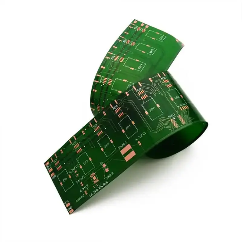
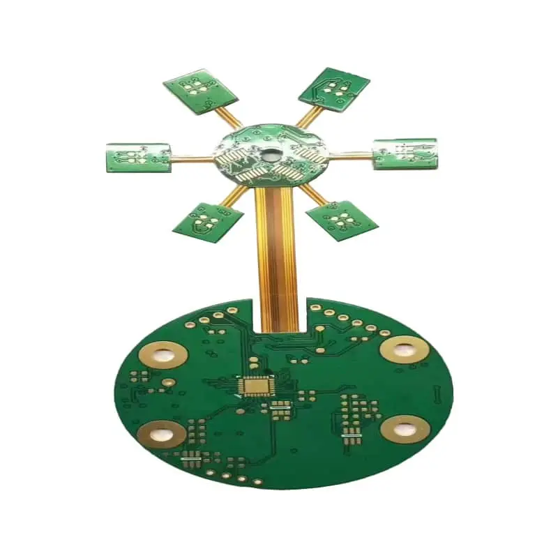
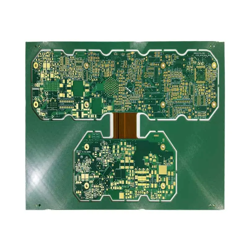
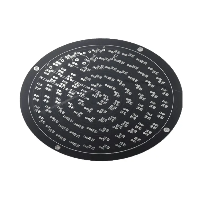
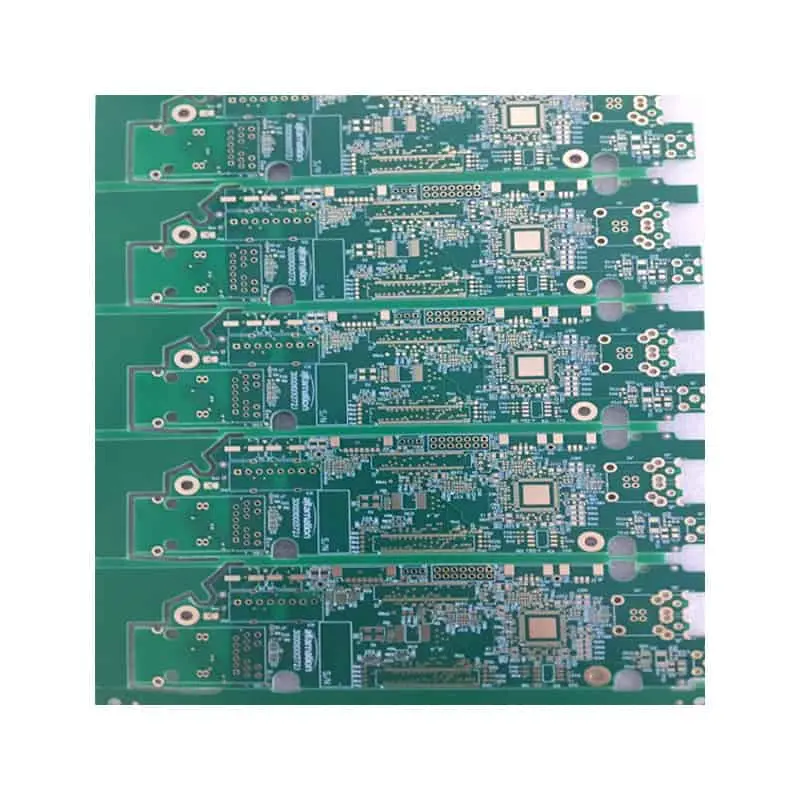
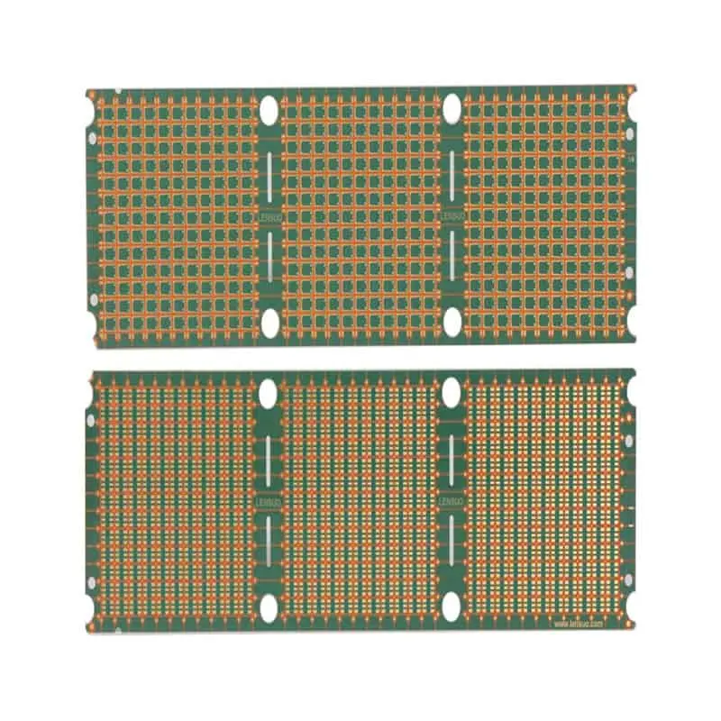
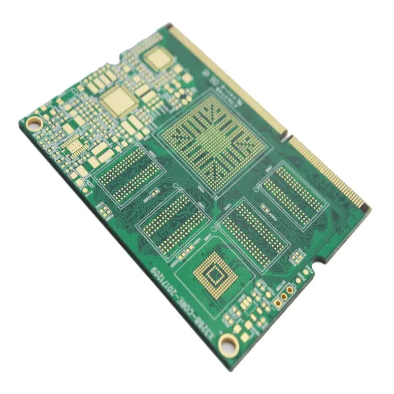
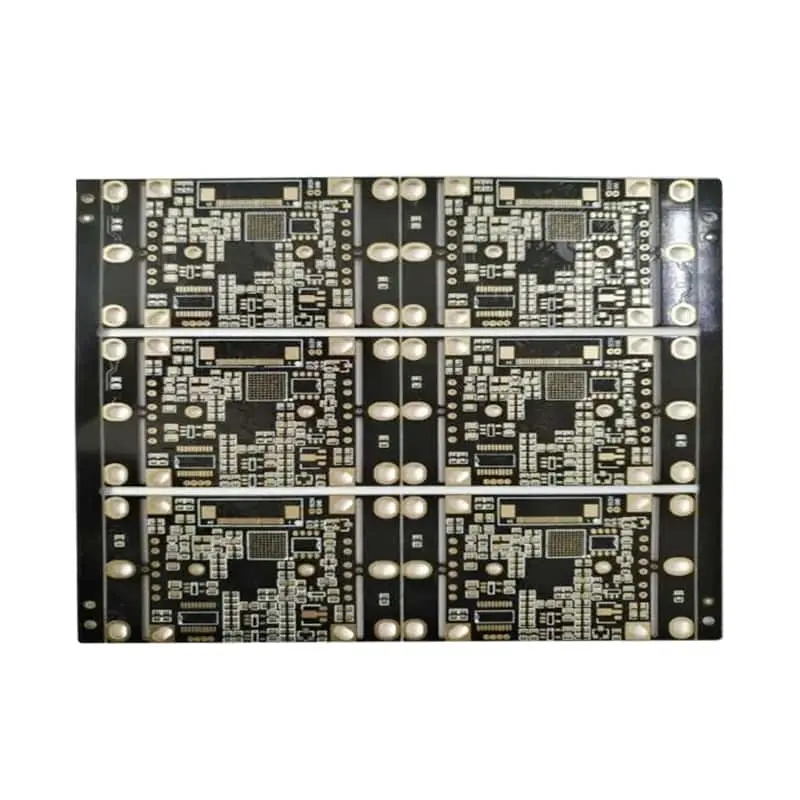
Rogers PCB manufacturing requires tighter control of dielectric properties, stackup geometry, copper features, via transitions, lamination, and impedance than standard FR-4 fabrication. For RF, microwave, and mmWave designs, choosing the right Rogers laminate is only the first step; the manufacturer must also prove material traceability, fabrication capability, impedance control, and test results.
What Should Engineers Consider When Choosing Rogers and Other High-Frequency Materials?

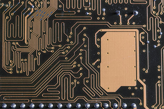
Rogers High-Frequency PCB Copper Traces and Substrate Macro View
Select the laminate according to operating frequency, dielectric loss, effective dielectric constant, thermal requirements, mechanical construction, and manufacturability—not simply the nominal Dk printed on a material datasheet.
For an RF PCB, the material decision affects insertion loss, phase stability, transmission-line dimensions, thermal behavior, and manufacturing yield. A material with excellent RF performance can still become a poor production choice if the fabricator cannot process its thickness, copper, bondply, or lamination structure consistently.
Common Rogers material options
Material family | Typical nominal Dk* | Typical low-loss Df* | Typical application |
|---|---|---|---|
RO4003C | ~3.38 | ~0.0027 | RF/microwave, antennas |
RO4350B | ~3.48 | ~0.0037 | RF amplifiers, power amplifiers, microwave |
RT/duroid 5870 | ~2.33 | ~0.0012 | High-frequency RF, antennas, mmWave |
RT/duroid 5880 | ~2.20 | ~0.0009 | Low-loss microwave and high-frequency links |
*Values are representative nominal material data and must be matched to the exact Rogers grade, test method, resin content, copper construction, and operating frequency used in the design.
One common engineering mistake is treating Dk as a single constant across every frequency. The effective Dk of an actual transmission line can differ from the laminate’s nominal datasheet Dk because field distribution, resin content, glass weave, conductor geometry, frequency, and stackup construction all contribute to the result.
For this reason, a manufacturer should be able to discuss:
- Dk and Df at the actual operating frequency
- laminate thickness tolerance
- resin content and cured dielectric thickness
- copper roughness
- glass-weave effects
- bondply compatibility
- surface-finish effects
- actual impedance coupon results
Which Rogers material fits which RF application?
Application | Preferred direction | Alternative direction |
|---|---|---|
Antenna feedline | RO4003C / RO4350B | RT/duroid series when lower loss is required |
RF filter | RO4350B | RO4003C |
RF power amplifier | RO4350B | RO4000-series alternatives |
Microwave/mmWave link | RT/duroid 5870/5880 | Low-loss RO4000-series material |
The correct choice should ultimately be confirmed against the RF model, frequency band, thermal environment, copper profile, and mechanical stackup.
What should procurement verify about Rogers material authenticity?
A purchasing team should request the exact manufacturer part number, material certificate, and batch traceability rather than accepting a quotation that simply states “Rogers material.”
For critical programs, verify:
- Original Rogers material part number
- Manufacturer or authorized distribution source
- Material thickness
- Copper foil type and thickness
- Lot/batch identification
- Certificate of Analysis (CoA), when applicable
- Approved substitute material, if any
This prevents a low-cost quotation from silently substituting a material with similar nominal Dk but different loss, thermal, or processing behavior.
How Should a Rogers PCB Stackup Be Designed for Controlled Impedance?
Build the stackup around the required 50 Ω single-ended or 100 Ω differential impedance, then control dielectric thickness, copper thickness, trace geometry, reference-plane continuity, and fabrication tolerances as one system.
A useful starting point is the transmission-line relationship:
Z₀ ≈ 87 / sqrt(εᵣ + 1.41) × ln( 5.98h / (0.8w + t) )
for a practical microstrip approximation, where:
h = dielectric height w = trace width t = copper thickness εr = dielectric constant
For production, however, this equation should be treated as a first-pass calculation, not the final impedance authority. The fabricator should use a validated field solver with the actual material construction.
Example controlled-impedance stackups
The following examples illustrate the engineering approach rather than prescribing universal production dimensions.
Board | Signal structure | Dielectric thickness | Copper | Initial trace target |
|---|---|---|---|---|
4-layer | Outer microstrip | ~0.10–0.15 mm | 35 µm | ~0.15–0.25 mm for 50 Ω |
6-layer | Inner stripline | ~0.10–0.15 mm | 35 µm | ~0.12–0.20 mm for 50 Ω |
8-layer | Inner differential stripline | ~0.08–0.12 mm | 35 µm | solver-controlled for 100 Ω pair |
These dimensions must not be copied directly into a production drawing. Rogers grade, actual cured dielectric thickness, copper profile, soldermask, trace etch compensation, and adjacent structures can change the final impedance.
For a supplier RFQ, specify:
- Target impedance: 50 Ω or 100 Ω differential
- Impedance tolerance: preferably ±5% where the design requires it
- Operating frequency
- Material grade
- Finished dielectric thickness
- Finished copper thickness
- Trace width/spacing
- Reference-plane configuration
- Via structure
- Backdrill requirements
- Surface finish
Why are via transitions critical on Rogers PCBs?
A via is not electrically invisible at high frequency.
Its pad, antipad, barrel, stub, and surrounding reference-plane geometry create parasitic capacitance and inductance. An unnecessarily long via stub can produce resonance and discontinuity.
For high-speed or microwave structures, engineers should evaluate:
- Via pad diameter
- Antipad diameter
- Drill diameter
- Finished hole
- Backdrill depth
- Stub length
- Ground-via spacing
- Reference-plane continuity
Microvias can reduce the electrical length of transitions, but they introduce manufacturing constraints involving laser drilling, copper plating, capture-pad size, stacking, and registration.
What happens when soldermask covers an RF trace?
Soldermask changes the electromagnetic environment around an exposed microstrip. Its dielectric contribution can shift the effective impedance and may increase loss.
For RF-sensitive traces, the design should explicitly state whether the impedance is calculated with:
- soldermask present,
- soldermask removed, or
- a controlled mask thickness.
This is a small drawing note that can prevent a surprisingly large engineering discussion during fabrication.
What Rogers PCB Fabrication Capabilities and Tolerances Should a Supplier Prove?
A qualified Rogers PCB manufacturer should demonstrate controlled capability for fine-line imaging, dielectric thickness, copper plating, registration, via formation, impedance, surface finish, and RF testing—not simply claim that it can “make Rogers PCBs.”
The critical fabrication parameters include:
Manufacturing characteristic | Typical engineering target |
|---|---|
Controlled impedance | ±5% for demanding RF designs |
Standard impedance | ±10% may be acceptable for less critical designs |
Fine trace/space | Defined by material, copper thickness, layer count and process |
Laser microvia | Capability depends on dielectric stackup and equipment |
Via aspect ratio | Must be matched to drill/plating capability |
Registration | Defined according to layer count and technology |
Plating thickness | Must meet drawing/IPC requirements |
Minimum annular ring | Defined by drill, pad and registration capability |
The key point for procurement is that a manufacturer’s advertised minimum capability is not automatically its stable production capability.
For example, a factory may state that it can produce a very small trace width, but the production question is whether it can maintain that geometry across the entire panel while simultaneously controlling copper thickness, etching, registration, and impedance.
What are the most important quality tests?
A serious RF PCB program should use a combination of electrical, dimensional, material, and reliability testing.
1. TDR impedance testing
Time-domain reflectometry can locate impedance discontinuities along a transmission line or test coupon.
It is particularly useful for identifying:
- trace-width variation
- dielectric-thickness variation
- connector/via transitions
- localized discontinuities
2. VNA testing
A vector network analyzer can characterize RF structures using parameters such as:
- S11
- S21
- return loss
- insertion loss
- phase response
For high-frequency designs, VNA verification can provide much more meaningful information than a basic continuity test.
3. AOI/FPI
Automated optical inspection or final visual inspection checks:
- open/short defects
- copper pattern defects
- registration problems
- soldermask defects
- pad damage
4. X-ray inspection
X-ray inspection is valuable for evaluating internal structures and plated features that cannot be visually inspected.
5. Thermal and environmental testing
Depending on the application, qualification may include:
- thermal cycling
- moisture absorption testing
- solderability
- thermal stress
- insulation resistance
- dielectric withstand
For aerospace, defense, medical, and other controlled applications, the manufacturer’s quality system and applicable IPC/UL/customer requirements must be established before production.
How should procurement read a Rogers PCB inspection report?
Do not accept a report simply because it contains a “PASS” stamp.
Ask the supplier to identify:
- PCB lot number
- Rogers material part number
- material batch
- test coupon identification
- impedance target
- measured impedance
- tolerance
- test method
- test equipment
- inspection quantity
- acceptance criteria
For critical characteristics, SPC or statistically defined sampling may be appropriate. This allows procurement and engineering teams to distinguish one successful sample from a repeatable manufacturing process.
How Much Do Rogers PCBs Cost and How Long Does Manufacturing Take?
Rogers PCB pricing is driven primarily by laminate cost, layer count, copper construction, fabrication complexity, testing, panel utilization, and production volume; RF prototype lead time can be significantly shorter than full-volume production when material is readily available.
A practical cost model is:
Total PCB Cost = Material + Lamination + Imaging/Etching + Drilling + Plating + Surface Finish + Testing + NRE + Scrap/Risk
Compared with conventional FR-4, Rogers laminates can carry a substantial material premium. The difference becomes more visible when the design uses:
- expensive low-loss laminate
- thick copper
- many layers
- hybrid Rogers/FR-4 construction
- sequential lamination
- laser microvias
- controlled impedance
- special surface finishes
- RF testing
What lead time should buyers expect?
For U.S.-market procurement planning, practical experience-based planning windows can be structured as:
Production stage | Planning window |
|---|---|
Fast prototype | 5–15 working days |
Small-batch pilot | 2–6 weeks |
Volume production | 6–12 weeks |
These are planning ranges, not guaranteed delivery times. Rogers material availability, laminate thickness, copper pricing, engineering review, tooling, testing requirements, and production capacity can move the actual schedule significantly.
How can procurement reduce Rogers PCB cost without sacrificing RF performance?
Three strategies are particularly effective.
Standardize stackups. If several products can share similar dielectric thicknesses and copper constructions, panel utilization and process setup can improve.
Approve alternatives before production. Do not wait until the preferred Rogers material is unavailable. Pre-qualify technically acceptable alternatives through engineering samples.
Separate prototype and mass-production requirements. A prototype may justify a faster, more expensive manufacturing route, while volume production should be optimized for stable yield and material availability.
For long-term programs, buyers should also discuss:
- EOL notification
- safety stock
- material batch traceability
- approved substitutes
- annual capacity
- price-adjustment mechanisms
- allocation during material shortages
What Should You Include When Requesting a Rogers PCB Manufacturing Quote?
Give the manufacturer enough RF and mechanical information to calculate material, process, impedance, testing, and lead-time requirements without making assumptions.
A high-quality RFQ should include:
- PCB layer count
- Board dimensions
- Rogers material and exact grade
- Operating frequency
- Target impedance
- Impedance tolerance
- Finished copper thickness
- Finished board thickness
- Trace/space requirements
- Via and microvia structure
- Surface finish
- Quantity
- Prototype or production requirement
- Required delivery date
- Gerber, ODB++, or complete fabrication data
For complex designs, include the stackup file and impedance requirements rather than asking the supplier to infer them from Gerbers.
A manufacturer should then be able to identify potential problems before fabrication, such as insufficient dielectric thickness, difficult via transitions, incompatible material combinations, or impedance targets that leave inadequate process margin.
How Should You Evaluate a Rogers PCB Manufacturer Before Placing a Production Order?
Evaluate the supplier on demonstrated process capability, RF test capability, material traceability, engineering support, quality documentation, and repeatability—not quotation price alone.
A useful supplier qualification checklist is:
Procurement question | What a strong supplier should provide |
|---|---|
Can you manufacture the specified Rogers grade? | Exact material confirmation |
Can you control 50 Ω / 100 Ω impedance? | Coupon/TDR results and tolerance |
Can you support RF testing? | TDR/VNA capability |
Can you trace material? | Lot/CoA documentation |
Can you handle complex stackups? | DFM/stackup engineering review |
Can you support prototypes? | Defined prototype process |
Can you support production? | Capacity and process controls |
Can you meet applicable standards? | Relevant quality documentation |
Can you manage material shortages? | Approved alternatives/supply strategy |
This approach is more reliable than selecting a supplier based only on a webpage claiming “Rogers PCB capability.”
What Should You Ask Before Choosing a Rogers PCB Supplier?
Ask questions that reveal whether the supplier can control RF performance repeatedly in production, not merely fabricate one prototype.
1. How do Rogers RO4350B and RT/duroid differ for RF designs above 10 GHz?
RO4350B is widely used for RF and microwave designs where a balance between electrical performance, thermal behavior, mechanical construction, and manufacturing practicality is required. RT/duroid materials are often selected when lower dielectric loss is a higher priority. The final choice should be based on the exact frequency, transmission-line structure, loss budget, and mechanical requirements.
2. What dielectric constant stability and loss tangent specifications should I use when modeling Rogers laminates?
Use the material data corresponding to the actual Rogers grade and test frequency, rather than treating one nominal Dk value as universally valid. For demanding designs, confirm how the manufacturer handles effective Dk, resin content, glass weave, copper roughness, and frequency-dependent loss.
3. What stackup and via-transition practices ensure controlled impedance for 50 Ω and differential pairs?
Maintain a continuous reference plane, control dielectric thickness, optimize trace width and spacing with a field solver, minimize unnecessary via stubs, and evaluate antipad and backdrill geometry. The final design should be validated through impedance coupons and, where appropriate, TDR or VNA testing.
4. What fabrication tolerances should I specify to keep impedance within ±5% on a high-frequency PCB?
Specify impedance tolerance explicitly and coordinate it with dielectric thickness, copper thickness, trace width, and registration tolerances. ±5% should be treated as a design/manufacturing target rather than an automatic capability claim; the supplier should demonstrate the result using representative coupons.
5. How do prototype costs and lead times compare with volume Rogers PCB production?
Prototypes commonly carry higher unit costs because material purchasing, tooling, engineering, and setup are distributed across fewer boards. A reasonable planning range is approximately 5–15 working days for fast prototypes, 2–6 weeks for small-batch pilot production, and 6–12 weeks for volume production, subject to material availability and technical complexity.
6. How can I verify authentic Rogers materials and authorized U.S. distributors?
Ask for the exact Rogers material designation and lot/batch traceability, then independently verify the supply chain through Rogers’ official distribution information or the distributor’s authorization documentation. For production programs, require the supplier to maintain material traceability from incoming laminate through the finished PCB.
Ready to Request a Rogers PCB Manufacturing Review?
The fastest way to determine manufacturability and pricing is to provide the PCB fabrication data together with the RF requirements, target impedance, material specification, quantity, and delivery requirement.
For a supplier evaluation or RFQ, a useful submission package includes:
- Gerber or ODB++
- Stackup specification
- BOM if assembly is required
- Target frequency
- 50 Ω / 100 Ω impedance requirements
- Impedance tolerance
- Rogers material grade
- Quantity
- Prototype or production volume
- Required delivery date
A qualified manufacturer can then review the design for stackup feasibility, impedance control, material availability, fabrication tolerances, testing requirements, cost, and lead time before production begins.
For sensitive RF designs, you can also request a pre-production DFM/stackup review and NDA/Confidentiality arrangement before releasing complete manufacturing data.
For an RF PCB quotation, the most useful RFQ fields are: Layer Count → Rogers Grade → Frequency → Impedance → Board Size → Quantity → Surface Finish → Lead Time → Testing Requirements.
About Author
David Chen https://www.linkedin.com/in/pcbcoming
David Chen boasts an extensive professional background in PCBA manufacturing, PCBA testing, and PCBA optimization, with specialized expertise in high-precision PCBA fault analysis and rigorous PCBA reliability testing. The author has worked with high-layer-count server PCB fabrication, ultra-low-loss backplane stackups, and thermo-mechanical reliability optimization for AI infrastructure projects involving 112G and 224G PAM4 architectures. Skilled in complex circuit design and cutting-edge advanced PCB manufacturing processes, he delivers solutions that elevate product durability and performance across industrial applications. His technical articles focusing on PCBA manufacturing workflows and testing methodologies are widely cited by industry peers, research institutions, and technical platforms, solidifying his reputation as a recognized technical authority in the global circuit board manufacturing sector.
David Chen https://www.linkedin.com/in/pcbcoming
David Chen boasts an extensive professional background in PCBA manufacturing, PCBA testing, and PCBA optimization, with specialized expertise in high-precision PCBA fault analysis and rigorous PCBA reliability testing. The author has worked with high-layer-count server PCB fabrication, ultra-low-loss backplane stackups, and thermo-mechanical reliability optimization for AI infrastructure projects involving 112G and 224G PAM4 architectures. Skilled in complex circuit design and cutting-edge advanced PCB manufacturing processes, he delivers solutions that elevate product durability and performance across industrial applications. His technical articles focusing on PCBA manufacturing workflows and testing methodologies are widely cited by industry peers, research institutions, and technical platforms, solidifying his reputation as a recognized technical authority in the global circuit board manufacturing sector.