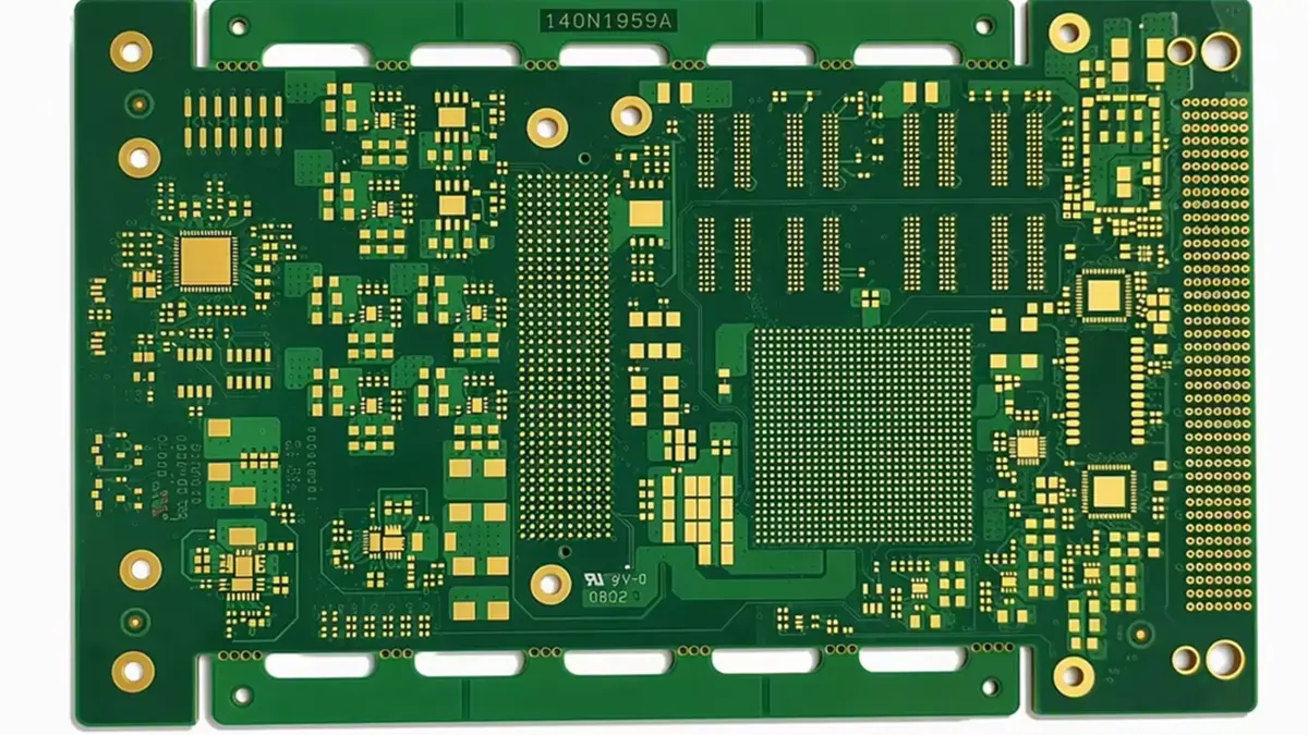
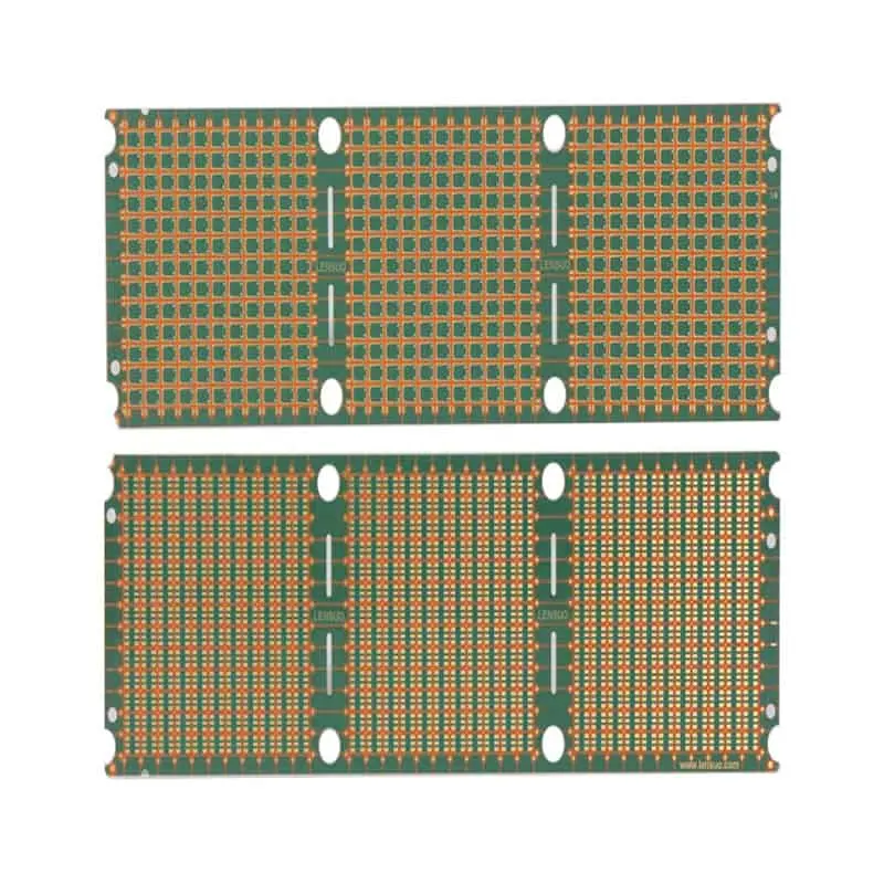
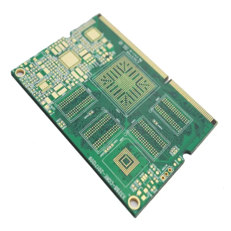
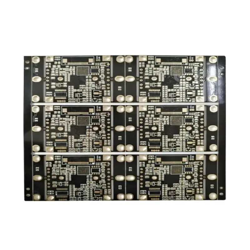
PCB laser etching uses a focused laser beam to selectively modify or remove material during printed circuit board manufacturing. Depending on the process, lasers can remove copper, pattern selected layers, or drill microvias. For OEM buyers, the right solution depends on copper thickness, substrate compatibility, feature size, registration accuracy, production volume, and total manufacturing cost—not simply the laser’s minimum spot size.
How Does PCB Laser Etching Work, and When Is It Better Than Chemical Etching?
 https://www.pcbcoming.com/product/
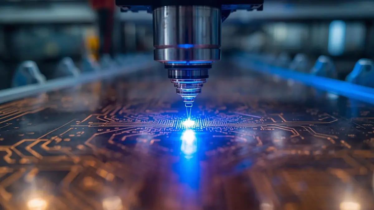
PCB Laser Etching Machine Processing High-Precision Circuit Patterns
PCB laser etching directs controlled laser energy onto selected areas of a copper-clad substrate to remove material or create defined features. It can be useful for rapid prototyping, localized material removal, specialized fine features, and applications where reducing wet-chemical processing is valuable. However, conventional chemical etching remains highly competitive for established PCB production processes and large production volumes.
What are the main steps in the laser etching process?
A typical laser ablation workflow follows these steps:
- CAM preparation: Convert approved Gerber or other manufacturing data into machine-readable toolpaths.
- Material preparation: Clean and secure the copper-clad laminate, flexible circuit material, or partially processed PCB.
- Optical alignment: Locate reference features and establish the coordinate system.
- Laser generation and focusing: Select the wavelength, pulse regime, energy density, and focus position appropriate for the material.
- Pattern processing: Use direct-write ablation or a compatible mask-assisted process to remove selected material.
- Cleaning and inspection: Remove debris, inspect the copper edges and substrate, and verify dimensional accuracy.
Direct-write processing eliminates the need for a physical pattern mask in the laser-writing step. Mask-assisted processing can be useful when a compatible mask improves selectivity or protects adjacent areas, although mask preparation and removal add operations.
How does laser processing compare with chemical etching?
| Evaluation factor | Laser ablation | Chemical etching |
|---|---|---|
| Pattern definition | Digital toolpath; no physical pattern mask required for direct writing | Usually requires imaging and resist processing |
| Feature selectivity | Depends on wavelength, fluence, pulse duration, and material response | Depends on resist pattern, chemistry, copper thickness, and etch control |
| Throughput | Can be limited by scanning distance and repeated passes | Well suited to panel-based processing |
| Chemical consumption | May reduce etchant use for the laser-treated operation | Requires controlled etching chemistry and associated rinsing |
| Main process risks | Heat damage, debris, uneven ablation, and copper-edge defects | Undercutting, over-etching, chemical control, and waste treatment |
| Best-fit applications | Specialized features, selected prototypes, and localized processing | Established production flows and high-volume circuit patterning |
Laser processing does not automatically eliminate chemical cleaning, plating, resist processing, or wastewater treatment elsewhere in PCB fabrication. For procurement decisions, compare the complete manufacturing route rather than one isolated operation.
Which Laser Types, Wavelengths, and Pulse Regimes Are Suitable for PCB Etching?
Laser selection should begin with the material being removed and the required feature quality. Wavelength determines how the copper and substrate absorb energy, while pulse duration and energy density influence removal efficiency, heat accumulation, and edge quality.
Which wavelengths are commonly used?
| Laser type | Representative wavelength | Typical engineering consideration |
|---|---|---|
| Infrared fiber or solid-state laser | 1,064 nm | Common industrial wavelength; reflective copper can complicate energy coupling |
| Green laser | 532 nm | May offer different copper absorption and processing behavior |
| Ultraviolet solid-state laser | 355 nm | Useful for precision micromachining when the material’s absorption characteristics are suitable |
| CO₂ laser | 10.6 µm | Widely associated with dielectric processing; copper removal behavior differs substantially from that of many polymer substrates |
| Ultrafast laser | Application-dependent | Picosecond and femtosecond systems can reduce heat diffusion under suitable conditions |
The laser’s nominal wavelength does not establish its ability to produce a specific trace width. Copper reflectivity, oxide condition, surface finish, beam quality, pulse energy, and substrate composition all affect the result.
How do pulse duration and spot size affect quality?
Continuous-wave (CW) lasers deliver energy continuously, whereas nanosecond, picosecond, and femtosecond lasers deliver energy in progressively shorter pulses. Pulsed systems can improve control over localized energy deposition, but short pulses alone do not guarantee defect-free processing.
For initial equipment screening, industrial micromachining systems may offer nominal focused spots ranging from approximately 10 to 100 µm, with actual values dependent on optics and beam configuration. Repetition rates can range from kilohertz operation to hundreds of kilohertz or higher. Fluence must be established experimentally for the particular copper, surface condition, and substrate.
Procurement teams should request measured spot size, pulse energy, repetition rate, scan speed, and validated processing windows—not just the equipment’s maximum power rating.
Which PCB Materials and Microvia Structures Can Laser Processing Handle?
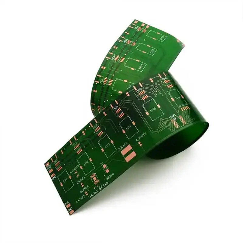
Laser processing can be applied to selected FR-4 laminates, high-frequency laminates, polyimide flexible circuits, and multilayer PCB structures. Compatibility depends on whether the operation targets copper, resin, reinforcement, coverlay, or another material. A recipe that works on one laminate or copper thickness may not transfer directly to another.
How should material and copper thickness influence process selection?
| Material or construction | Key engineering concern | Recommended validation |
|---|---|---|
| FR-4, standard Tg grades | Resin damage, glass-fiber exposure, and debris | Inspect the ablated edge and dielectric surface |
| High-Tg FR-4 | Resin response and compatibility with the complete thermal process | Test the actual laminate grade and stackup |
| Rogers or other RF laminates | Different dielectric chemistry and copper surface characteristics | Confirm substrate integrity and RF-critical geometry |
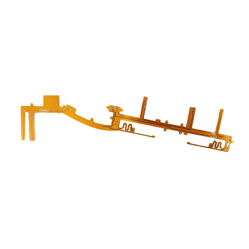
| Polyimide flexible circuits | Dimensional movement, local heating, and film damage | Test on the actual flexible construction |
| 1 oz copper, approximately 35 µm nominal | Removal depth and remaining-copper control | Verify copper removal and edge dimensions |
| 2 oz copper, approximately 70 µm nominal | Higher material-removal demand and possible heat accumulation | Validate the number of passes and cycle time |
These copper thicknesses are nominal references, not guaranteed final thicknesses. Actual foil specifications and processed copper geometry must be confirmed.
How are laser-drilled microvias different from laser-etched copper traces?
Laser-drilled microvias connect PCB layers by removing dielectric material to create small holes, typically followed by desmear, metallization, and copper plating. Laser etching, by contrast, removes selected material to form a pattern or feature. A laser capable of drilling a microvia does not necessarily have the correct process window for fine copper circuit ablation.
Microvia diameters around 50–150 µm are common in advanced PCB manufacturing, although achievable dimensions depend on the dielectric, copper configuration, laser system, and downstream processing. Aspect ratios near 0.75:1 to 1:1 are useful initial discussion points for some microvia constructions, not universal limits.
For multilayer boards, manufacturers must also control layer registration, via-to-capture-pad alignment, resin residue, plating integrity, and thermal rel.
About Author
David Chen LinkedIn Profile
David Chen is a Senior RF/PCB Process Engineer at Shenzhen Hongda Circuit Technology Co., Ltd., with over 12 years of experience in high-frequency PCB fabrication, impedance-controlled stack-up design, and Rogers/PTFE laminate processing. He also boasts an extensive professional background in PCBA manufacturing, PCBA testing, and PCBA optimization, with specialized expertise in high-precision PCBA fault analysis and rigorous PCBA reliability testing. The author has worked with high-layer-count server PCB fabrication, ultra-low-loss backplane stackups, and thermo-mechanical reliability optimization for AI infrastructure projects involving 112G and 224G PAM4 architectures. Skilled in complex circuit design and cutting-edge advanced PCB manufacturing processes, he delivers solutions that elevate product durability and performance across industrial applications. His technical articles focusing on PCBA manufacturing workflows and testing methodologies are widely cited by industry peers and technical platforms, and have gained attention and recognition from industry colleagues.