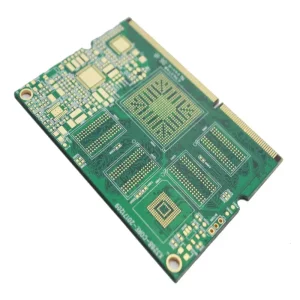
12 Layers Blind And Buried Via Hole PCB
Blind PCB can achieve more efficient circuit connections, reduce placing space, and improve the performance and reliability of the circuit board.Blind and buried holes can add more connection points to the circuit board, reduce noise and electromagnetic interference in the circuit board, and improve the reliability and stability of the circuit board. High -quality signal transmission avoids the circuit board interruption due to excessive pressure or vibration.
Share to:
| Key attributes |
| Industry-specific attributes |
| Base Material:FR4 |
| Board Thickness:1.6mm |
| Other attributes |
| Copper Thickness:1 oz |
| Min. Hole Size:3 mil |
| Min. Line Width:3 mil |
| Min. Line Spacing:3 mil |
| Surface Finishing:Lead Free HASL |
| Copper Thickness: |
| Layers:1-28L |
| Finished board thickness:0.2-7.0mm |
| Finised copper thicckness:1-6OZ |
| Board thickness tolerance:+/-10% |
| Hole tolerance: PTH: +/-3mil NPTH: +/-2mil |
| Min distance pad-pad:8mil |
| PCB Standard:IPC-A-610 D/E |
| Packaging and delivery |
| Package Type:1. at buyer’s request 2. inner, vacuum package 3. outer, standard export carton. |
| attribute-list |
| Supply Ability:500000 Square Centimeter/Square Centimeters per Month PCB Factory |