How Much Do Custom PCBs Cost and How Long Do They Take From China to the U.S.?
A simple 2-layer prototype can be budgeted from roughly $20–$80 for 1–10 boards, while a 6-layer prototype commonly requires $80–$250+, depending on dimensions, material, copper weight, finish, drilling, impedance control, and engineering requirements. These are budgetary planning ranges, not fixed quotations. Production quantities normally reduce PCB cost substantially, but freight, tooling, testing, and special materials can change the landed cost.
For U.S. procurement, separate fabrication lead time from transit time:
| Example | Prototype quantity | Budgetary PCB cost* | Typical fabrication planning window | Express delivery planning |
|---|---|---|---|---|
| 2-layer FR-4 | 1 pc | $20–$50 | 3–7 working days | ~2–4 days transit |
| 2-layer FR-4 | 10 pcs | $25–$80 total | 3–7 working days | ~2–4 days transit |
| 2-layer FR-4 | 100 pcs | $60–$180 total | 5–10 working days | ~2–4 days transit |
| 6-layer FR-4 | 1 pc | $80–$180 | 7–12 working days | ~2–4 days transit |
| 6-layer FR-4 | 10 pcs | $100–$250 total | 7–12 working days | ~2–4 days transit |
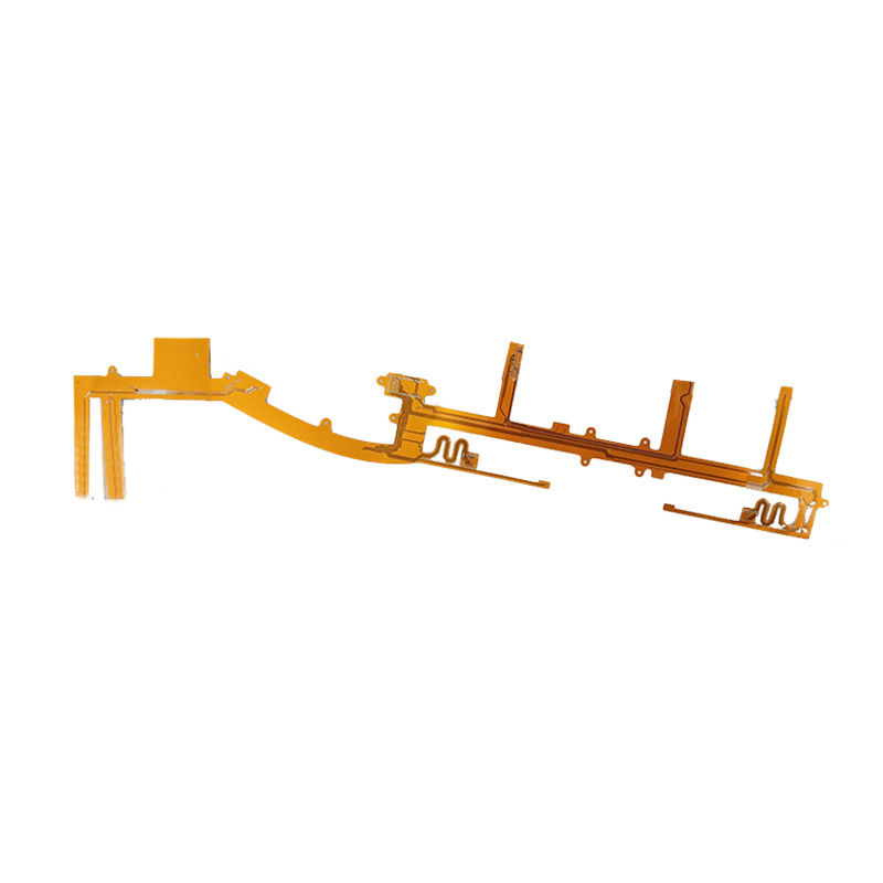
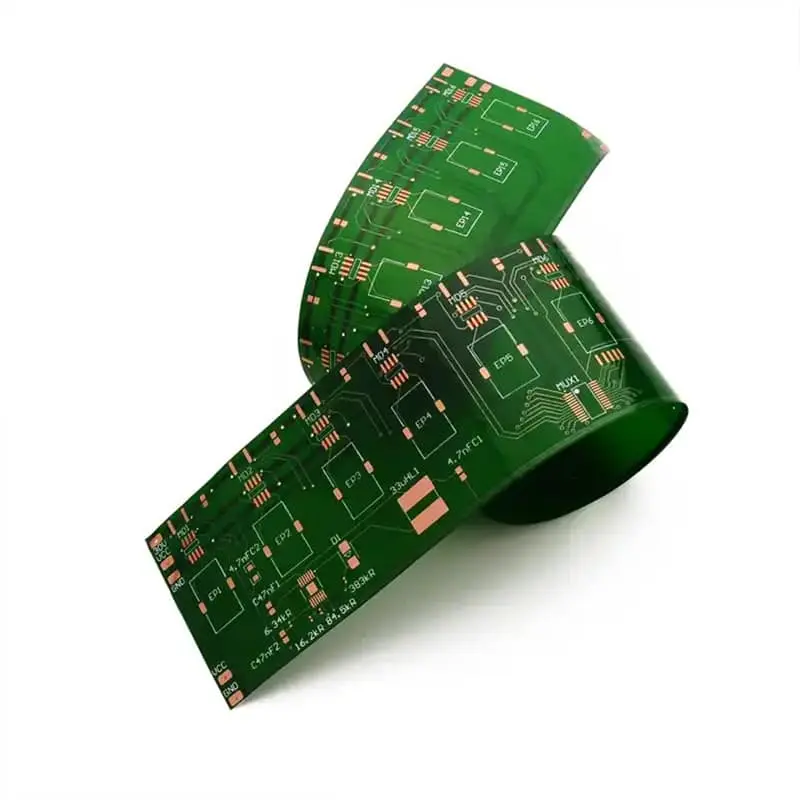
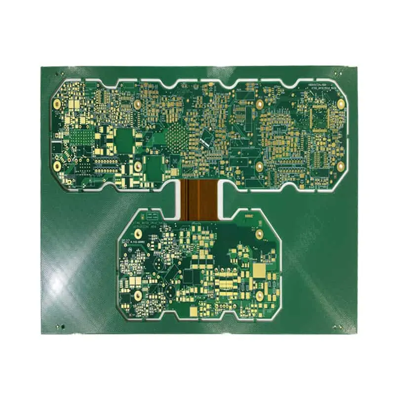
| Flexible PCB | 10 pcs | $80–$250+ total | 7–15 working days | ~2–4 days transit |
*Illustrative procurement-planning ranges only. Actual pricing must be calculated from the released Gerber/ODB++, stackup, quantity, material, copper weight, finish, tolerances, testing, and delivery terms.
A useful quote should expose the cost structure rather than simply stating a unit price:
PCB price = fabrication + engineering/NRE + tooling + testing + packaging + freight + applicable duties/taxes.
For example, a 100-piece six-layer board may have a relatively low bare-board unit cost, but adding ENIG, 2 oz copper, impedance coupons, controlled-depth backdrilling, laser microvias, or special high-frequency laminate can change the economics significantly.
The main manufacturing pain point is usually not the nominal PCB price. It is cost escalation after engineering review. A board quoted on standard FR-4 may become substantially more expensive after the factory discovers a high layer count, unusually small annular rings, tight registration requirements, low-Dk laminate, heavy copper, or sequential lamination.
For U.S. landed cost, do not assume that “DDP” automatically means a fixed tariff percentage. U.S. treatment is based on the applicable HTS classification and current trade measures; USTR specifically directs importers to determine the HTS subheading before determining additional Section 301 duty.
A practical RFQ should therefore request EXW/FOB, DDP and freight-only numbers separately whenever possible.
What Manufacturing Capabilities Should a Custom PCB Manufacturer in China Provide?

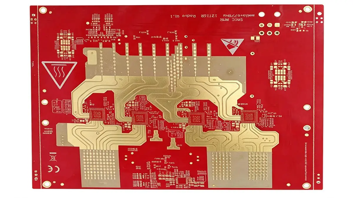
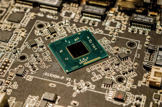
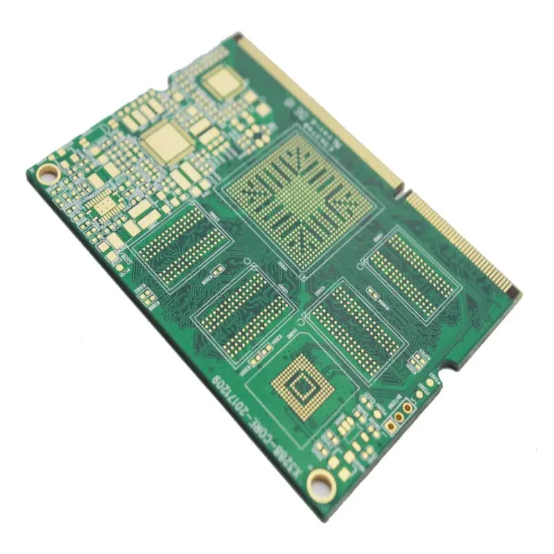
Precision Macro View of Complex Multi-layer Custom PCB with HDI
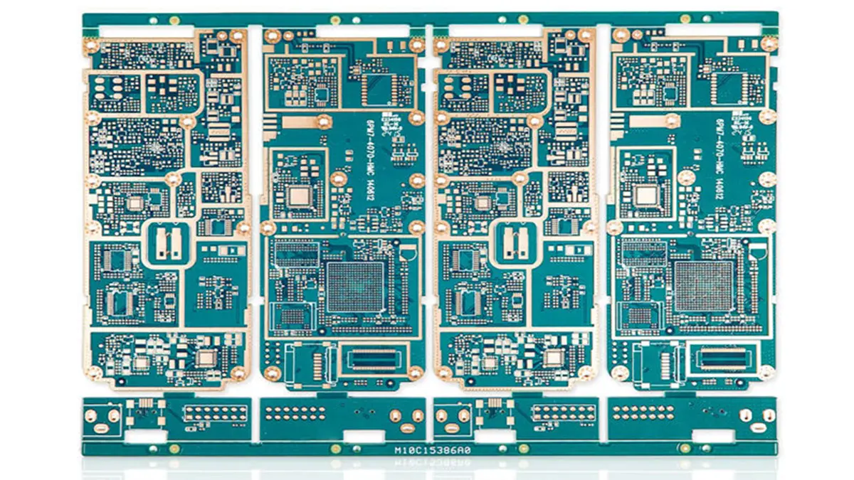
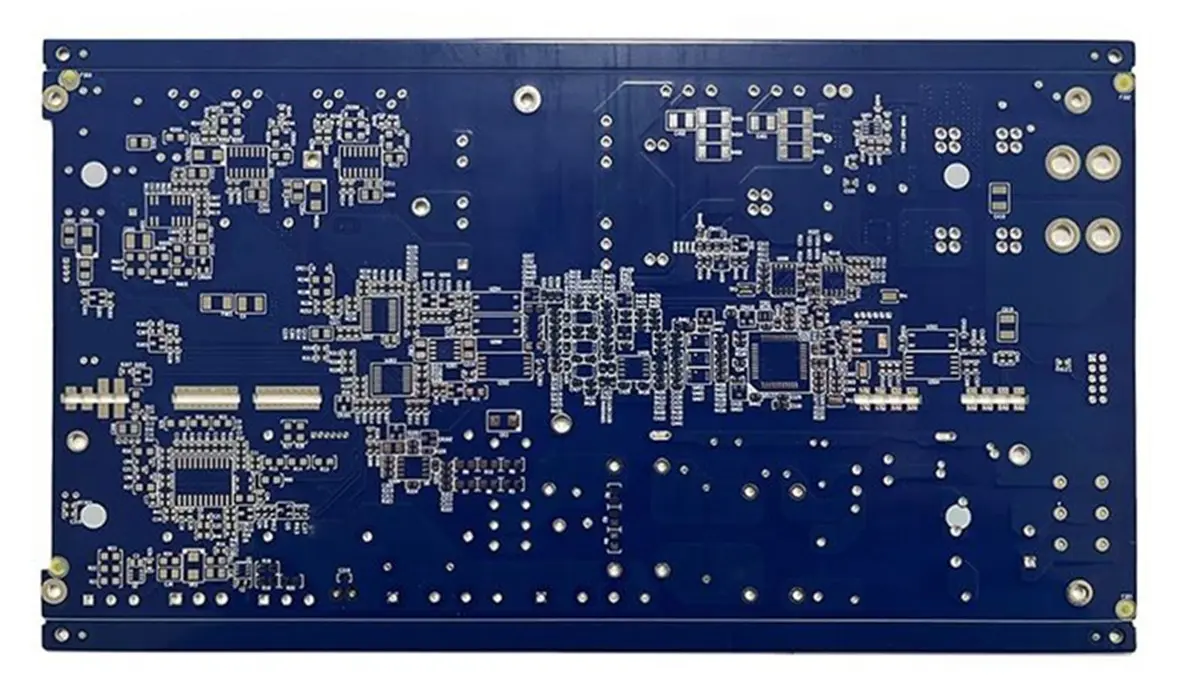
A serious custom PCB supplier should match the board architecture to its qualified process platform, not advertise one universal “minimum line/space” number. Typical procurement specifications should cover multilayer construction, flex and rigid-flex, blind/buried vias, microvias, copper thickness, laminate selection, impedance control, and finished-board tolerances.
For example, a conventional 6-layer high-speed FR-4 design might use:
| Layer | Function | Example construction |
|---|---|---|
| L1 | Components / high-speed signals | Microstrip |
| L2 | Solid GND | Reference plane |
| L3 | High-speed signals | Stripline |
| L4 | High-speed signals | Stripline |
| L5 | Power / GND | Plane |
| L6 | Components / signals | Microstrip |
For a 50 Ω single-ended or 90/100 Ω differential interface, the manufacturer should calculate the actual trace width, spacing, dielectric thickness and copper thickness from the released stackup, rather than applying a generic online calculator value.
For example, a 100 Ω differential pair may require:
- controlled dielectric thickness between signal and reference plane;
- matched differential geometry;
- consistent copper thickness;
- controlled resin content after lamination;
- registration control between layers;
- impedance test coupons;
- TDR verification where specified.
The same principle applies to HDI. IPC-6012F explicitly covers multilayer boards with PTHs and structures involving buried, blind and microvias, while its 2023 revision expanded attention to microvia reliability, internal plated layers, hole registration and dielectric spacing.
Typical material selection
FR-4: economical choice for general digital, industrial and control electronics.
High-Tg FR-4: useful where thermal cycling, lead-free assembly or higher operating temperatures increase reliability requirements.
Rogers/high-frequency laminates: appropriate when dielectric loss, Dk stability and RF performance become important.
Polyimide: commonly selected for flexible circuits where repeated bending, thin construction or dynamic flexing is required.
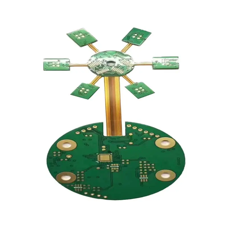
Rigid-flex: useful when connectors, cable harnesses and multiple interconnects can be eliminated by integrating the flexible section into the PCB structure.
The engineering pain point is over-specification at quotation stage and under-specification at production stage. A buyer may request “high precision” without defining finished copper, hole tolerance, impedance tolerance, dielectric thickness, surface finish, or IPC class. The supplier then makes assumptions, and the assumptions become the source of later disputes.
An experienced engineering review should therefore convert vague requirements into measurable manufacturing characteristics.
How Should Turnkey PCB Assembly, Quality Control and Certifications Be Verified?
Turnkey PCBA should be controlled as a traceable manufacturing process: BOM sourcing → incoming inspection → SMT → reflow → AOI → X-ray where required → THT → electrical testing → functional testing → final inspection → batch records → shipment.
A procurement team should not accept “100% quality inspection” as sufficient evidence. Ask what was inspected, by which method, against which acceptance criteria, and whether the records are available by lot or serial number.
| Control point | Typical evidence to request |
|---|---|
| Incoming PCB | IQC record / dimensional inspection |
| Components | Part number, manufacturer, lot/date code |
| SMT | SPI/AOI records where applicable |
| BGA/QFN | X-ray inspection sample or report |
| Through-hole | Visual / solder-joint inspection |
| Electrical | ICT or flying-probe report |
| Product operation | Functional test record |
| Final release | Final inspection / OQC record |
| Traceability | Batch, work order, operator/process records |
AOI is particularly useful for solder bridges, missing components, polarity errors and placement defects. X-ray becomes important where solder joints are hidden under BGA, QFN or bottom-terminated packages. ICT/flying-probe testing addresses electrical connectivity, while functional testing verifies the product’s actual operating behavior.
For rigid boards, IPC-6012F is the current IPC qualification and performance specification identified by IPC for rigid printed boards. IPC also identifies IPC-6013 for flexible printed boards.
For assembly acceptance, the procurement specification may also reference IPC-A-610 and J-STD-001, depending on the product and customer requirements. IPC’s current standards resources list IPC-A-610J and J-STD-001J among recently published assembly standards.
For compliance, buyers should distinguish between:
- ISO 9001 — quality management system;
- RoHS/REACH declarations — material/substance compliance;
- UL recognition/listing — applicable only where the relevant PCB construction and certification scope are covered;
- IPC Class 2/3 — product acceptance/performance classification, not a generic factory certification;
- CE — generally relates to the finished applicable product’s regulatory conformity rather than simply proving that a bare PCB factory is “CE certified.”
That distinction matters during supplier audits. A certificate without its scope, issuing organization, validity period and covered product/process is weak evidence.
How Can a PCB Manufacturer Scale NPI to Mass Production While Protecting IP?
The safest NPI route is to divide production into controlled gates: DFM review → prototype → engineering validation → pilot build → FAI/first-article approval → reliability validation → production release → controlled ramp.
A practical 6-stage schedule is:
- Day 0–2 — Engineering review: Gerber/ODB++, BOM, drawings, stackup, impedance requirements and test specifications.
- Day 3–10 — Prototype fabrication: validate dimensions, drilling, stackup, solderability and electrical performance.
- Day 11–15 — Assembly validation: SMT/THT process verification and functional testing.
- Week 3–4 — Pilot build: controlled quantity with production-intent materials and process parameters.
- Week 4–6 — FAI/reliability release: approve first article, inspection records and test results.
- After approval — Volume ramp: freeze revision, BOM and approved manufacturing instructions.
The exact duration depends on board complexity and the customer’s validation requirements.
Where NPI commonly fails
One recurring failure mode is prototype-to-production process substitution. A prototype may use one laminate lot, one copper foil construction and one drilling recipe, while volume production uses another qualified process. If those substitutions are not documented, the buyer can experience impedance variation, registration changes, solderability problems or yield loss during ramp-up.
Another common problem is BOM instability. An assembler may quote an attractive turnkey price based on nominal manufacturer part numbers but later substitute components because of availability. For a controlled product, substitutions should require explicit customer approval.
IP protection should be procedural, not verbal
For proprietary designs, buyers can require:
- NDA before engineering review;
- controlled access to design files;
- customer-specific internal part numbers;
- revision-controlled manufacturing packages;
- restricted access to BOM and Gerber files;
- written rules for subcontracting;
- prohibition of unauthorized sample reuse;
- controlled disposal of obsolete documents;
- approval before component substitutions.
A factory audit should cover quality, production, ESD controls, material storage, traceability, subcontractors, cybersecurity/document access, worker safety and business continuity, not just factory size.
For U.S. customers, the objective is not simply finding the cheapest PCB factory. It is establishing a repeatable manufacturing system in which the same design revision produces the same electrical and mechanical result across multiple lots.
What Files and DFM Information Are Needed for a Fast, Accurate PCB Quote?
The fastest RFQ normally includes Gerber or ODB++ files, stackup, PCB drawing, BOM, assembly drawing, quantity, target delivery date, material, copper weight, surface finish, testing requirements and destination.
RFQ checklist
Bare PCB
- Gerber/ODB++ manufacturing files
- PCB dimensions
- layer count
- finished thickness
- copper weight
- material/Tg requirement
- surface finish
- solder mask and silkscreen
- minimum line/space
- minimum finished hole
- blind/buried/microvia requirements
- controlled impedance requirements
- IPC class
- quantity and panelization preference
PCBA
- BOM with manufacturer part numbers
- centroid/pick-and-place file
- assembly drawing
- polarity information
- test requirements
- programming requirements
- functional test procedure
- approved alternate parts
- component lifecycle constraints
- packaging requirements
The DFM report should not simply say “pass.” It should identify the exact feature, measured/required value, proposed correction and manufacturing consequence.
For example:
Requirement: 0.10 mm trace/space
Manufacturing concern: feature is below the supplier’s standard qualified production rule for the selected copper/stackup
Engineering action: review mSAP/subtractive process option or relax geometry
Commercial impact: potential NRE/process premium and yield impact
This is much more useful to an engineer than a generic “DFM issue.”
Surface finish should also be selected according to application rather than price alone:
| Finish | Typical consideration |
|---|---|
| HASL | Economical; less suitable for very fine-pitch flatness requirements |
| Lead-free HASL | Common RoHS-oriented option; thermal process involved |
| ENIG | Flat surface, widely used for fine-pitch SMT and edge-contact applications |
| OSP | Cost-effective flat finish; handling/storage considerations apply |
The deeper manufacturing issue is that DFM begins before fabrication. IPC itself describes DFM as an important design-stage activity and provides DFM profiles spanning different performance classes and producibility levels.
For a U.S. procurement engineer, a valuable DFM review should therefore answer three questions:
Can you manufacture it?
Can you manufacture it repeatedly?
What design change would reduce cost or manufacturing risk without compromising function?
That third question is where experienced PCB engineering support creates measurable value.
Why Choose HAODA ELECTRONIC CO.,LIMITED. for Custom PCB Manufacturing in China?
The appropriate supplier should be evaluated on engineering responsiveness, documented process capability, inspection evidence, NPI control, communication and landed cost—not on the lowest initial PCB quotation alone.
For a U.S. project, HAODA ELECTRONIC CO.,LIMITED can structure an RFQ around the actual engineering package rather than a generic “PCB price.”
The recommended procurement package is:
Gerber/ODB++ → DFM review → engineering questions → prototype quotation → production quotation → inspection/test requirements → NPI approval → controlled production → U.S. delivery.
Buyers can also request supporting evidence such as:
- sample AOI records;
- X-ray inspection examples;
- ICT/flying-probe test records;
- dimensional inspection records;
- material certificates;
- IPC acceptance criteria;
- quality-system certificates;
- factory audit documentation;
- traceability examples.
For confidential designs, an NDA can be arranged before detailed technical files are exchanged.
Request a custom PCB quotation with your Gerber files, BOM, quantity and target delivery date. A useful first quotation should show not only the board price, but also the assumptions behind material, stackup, surface finish, testing, tooling, lead time and shipping.
For U.S. deliveries, ask for the commercial term explicitly—EXW, FOB, DDU/DAP or DDP—and request the estimated landed-cost components separately. This is particularly important because U.S. tariff treatment can change according to HTS classification and applicable trade actions or exclusions.
FAQ: What Do U.S. Buyers Need to Know Before Choosing a Custom PCB Manufacturer in China?
1. How long does a prototype PCB typically take to arrive in the U.S.?
For a straightforward prototype, a practical planning assumption is approximately 3–10 working days for fabrication, followed by roughly 2–4 days of express international transit, depending on board complexity, production queue and destination. Complex multilayer, HDI, flex, rigid-flex or special-material boards can require longer fabrication.
The important distinction is between factory lead time and transportation time. Always request both separately.
2. What will a 2-layer or 6-layer prototype cost at quantities of 1, 10 and 100?
A simple 2-layer FR-4 prototype may fall into a budgetary range of approximately $20–$80 for 1–10 pieces, while 100 pieces may reduce the effective board cost substantially. A 6-layer prototype can commonly require approximately $80–$250+ for 1–10 pieces, depending on construction.
These figures are planning examples, not guaranteed market prices. Dimensions, copper weight, material, surface finish, drilling, impedance control and testing can move the quotation significantly.
3. What MOQ should I expect from a Chinese PCB manufacturer?
PCB fabrication does not necessarily require a traditional high MOQ. Prototype orders can be as small as 1–10 boards, while production economics usually improve at higher quantities. Flex and rigid-flex may have additional tooling or engineering charges even when the PCB quantity itself is small.
The better RFQ question is therefore not simply “What is your MOQ?” but “What are your NRE, tooling and unit-cost changes at 1, 10, 100, 1,000 and 10,000 pieces?”
4. Which QC tests and certifications should I request?
For bare boards, consider dimensional inspection, visual inspection, microsection where applicable, electrical testing and impedance testing. For assemblies, AOI, X-ray, ICT/flying-probe and functional testing should be selected according to product risk.
For rigid PCBs, IPC-6012F is the relevant IPC qualification/performance specification; IPC identifies IPC-6013 for flexible printed boards.
Request the actual scope and validity of ISO certificates and compliance documents rather than accepting a certificate logo on a supplier website.
5. How should a PCB project move from prototype to mass production?
Use a controlled NPI process: DFM → prototype → validation → pilot build → FAI → reliability/functional approval → production release.
Freeze the PCB revision, BOM, approved alternates, manufacturing drawings, test procedures and acceptance criteria before volume production. For proprietary products, establish an NDA and document controls before releasing sensitive engineering files.
About Author
David Chen https://www.linkedin.com/in/pcbcoming
David Chen is a Senior RF/PCB Process Engineer at Shenzhen Hongda Circuit Technology Co., Ltd., with over 12 years of experience in high-frequency PCB fabrication, impedance-controlled stack-up design, and Rogers/PTFE laminate processing. He also boasts an extensive professional background in PCBA manufacturing, PCBA testing, and PCBA optimization, with specialized expertise in high-precision PCBA fault analysis and rigorous PCBA reliability testing. The author has worked with high-layer-count server PCB fabrication, ultra-low-loss backplane stackups, and thermo-mechanical reliability optimization for AI infrastructure projects involving 112G and 224G PAM4 architectures. Skilled in complex circuit design and cutting-edge advanced PCB manufacturing processes, he delivers solutions that elevate product durability and performance across industrial applications. His technical articles focusing on PCBA manufacturing workflows and testing methodologies are widely cited by industry peers and technical platforms, and have gained attention and recognition from industry colleagues.