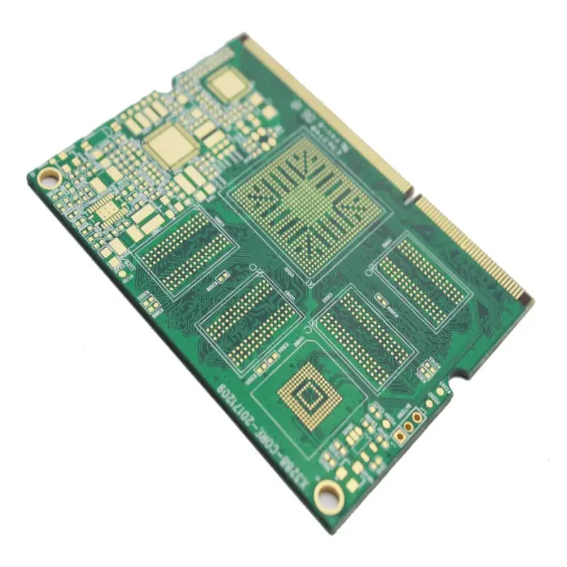
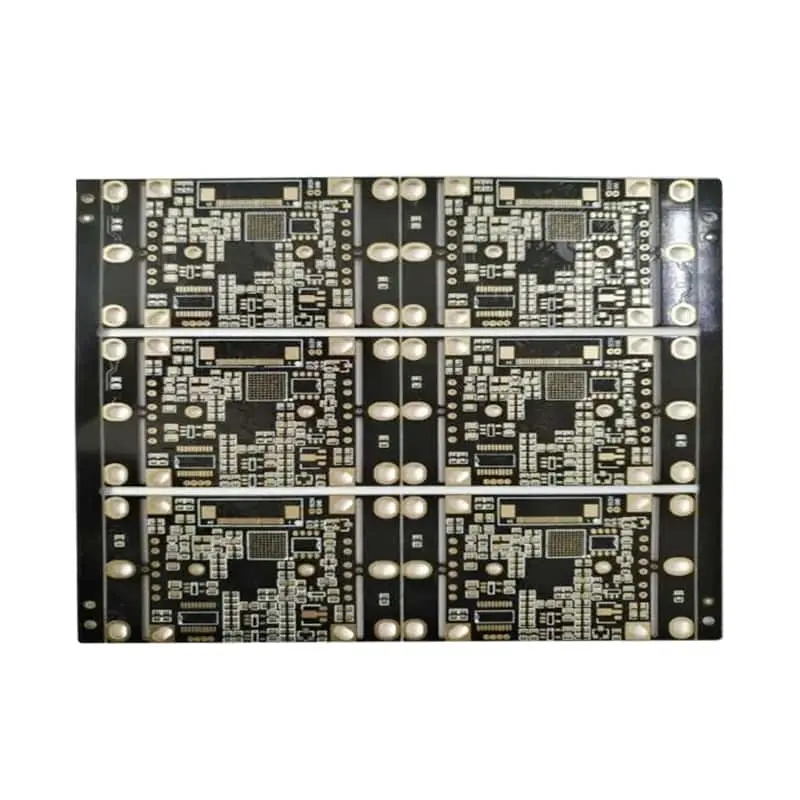
PCB manufacturing supplier selection matters greatly whether you’re sourcing boards for a consumer wearable, an automotive ECU, or an aerospace program. The ideal partner stands out based on five key factors: realistic lead times, transparent pricing, verified technical capability, documented quality, and a disciplined NPI workflow. Here is exactly what to evaluate — and what questions to ask — before you send out your Gerbers.
Lead Times, Turnarounds, and Rush Options
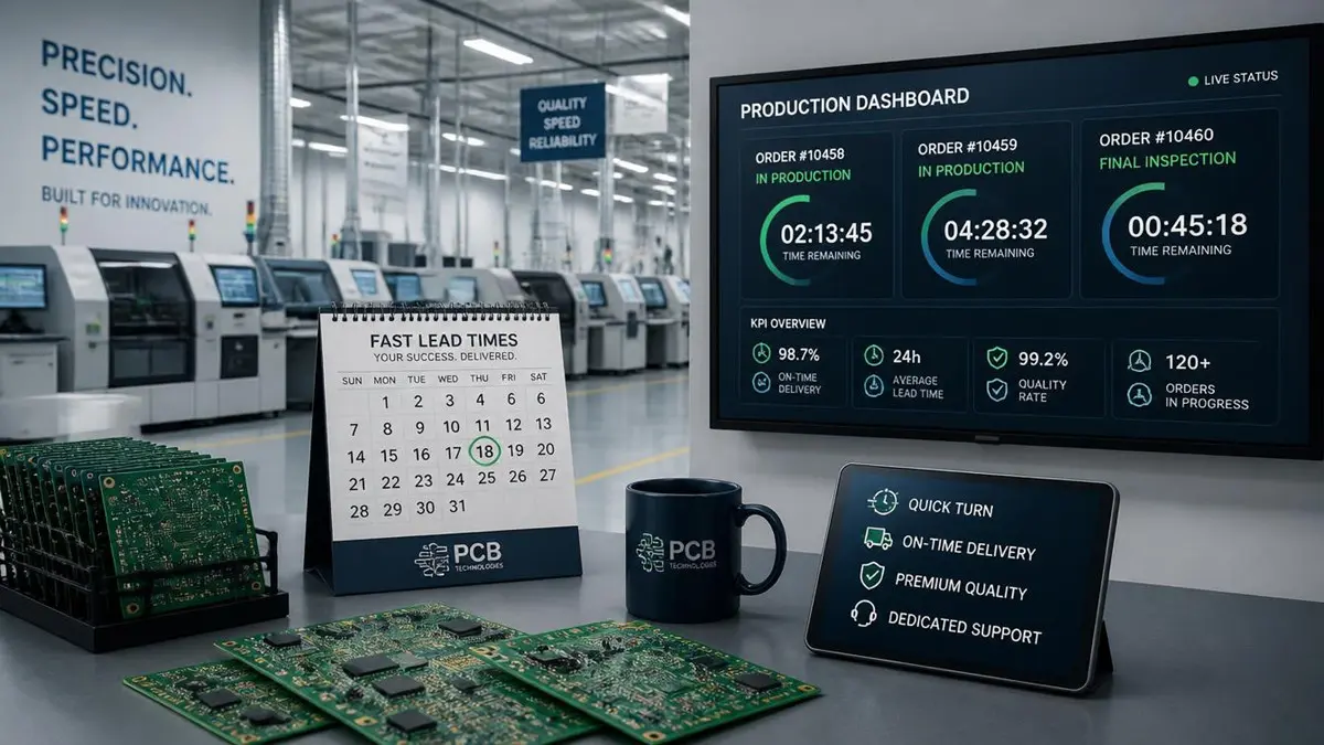
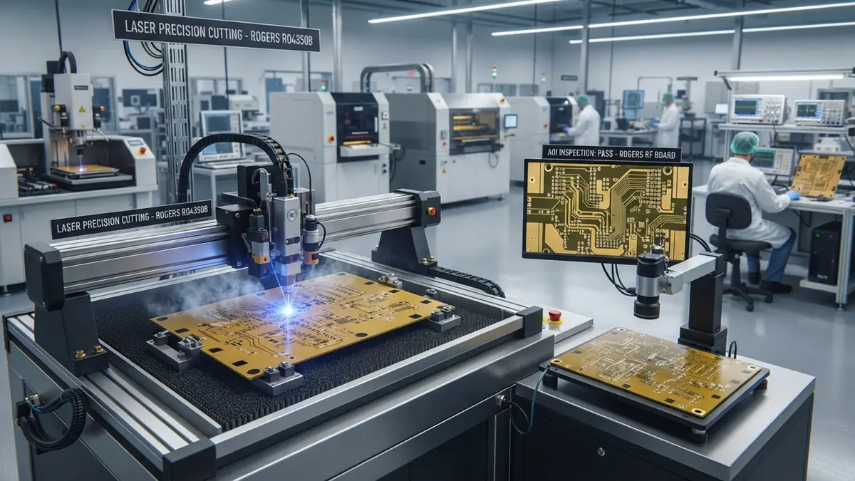
A professional pcb manufacturing supplier utilizing a digital production dashboard and real-time countdown tracking to ensure fast and reliable lead times.
Lead time depends primarily on order size and where the boards are built. For prototypes, domestic U.S. quick-turn shops typically deliver in 3–5 business days, while offshore fabrication runs 8–12 working days plus 15–30 days of ocean freight — customs clearance and port congestion can add another week. Small-batch production (50–500 units) usually takes 5–10 days domestically versus 3–5 weeks door-to-door offshore. Volume orders range from 2–4 weeks at U.S. fabs to 6–10 weeks from Asia.
Within any quote, four factors move the date: material shortages (especially high-Tg laminates), layer count (an 8-layer board ships 2–3 days slower than a 2-layer), surface finish (ENIG adds 1–2 days versus OSP or lead-free HASL), and test level (full flying-probe or ICT coverage adds 1–3 days depending on net count).
To predict a firm delivery date, work backward from your need-by date in the supplier’s delivery calculator: fabrication days + one day of engineering review for new panels + test and assembly days + transit time by ZIP code. For time-critical U.S. distribution, expedited paths include domestic quick-turn lines (a 30–50% premium), weekend and night-shift processing, and split shipments — part by air, balance by sea. For retail launches and defense or ITAR-controlled programs, domestic-only builds remove customs risk entirely, typically at a 20–40% cost premium.
Transparent Pricing, Quotes, and Minimum Order Quantities
A quote you can compare line by line should itemize: base material and thickness, layer count, surface finish (ENIG, immersion silver, OSP, HASL), drill charges including blind and buried vias, electrical testing, assembly labor, components if turnkey, packaging, freight, and duties. Suppliers confident in their pricing publish a downloadable price matrix and a freight calculator with region-specific U.S. estimates.
MOQs shift with volume and service scope. For fabrication only, prototype shops accept 1–5 pieces at $50–$500 per board; small-batch runs start at 10–50 pieces; volume pricing typically kicks in at 100+ panels. For turnkey assembly, MOQs are often driven by component reels — a single line setup may require 25–100 boards to be economical. Always request the full quantity-break table rather than a single price point: unit cost routinely drops 40–60% between 10 and 500 units, and assembly setup fees amortize quickly above a few hundred boards.
Real negotiation levers: consolidate multiple designs onto one panel and one purchase order, swap ENIG for OSP on boards that will be assembled within weeks, and re-optimize your stackup to eliminate unneeded layers. To expose hidden fees, ask specifically about NRE and tooling, setup charges, test-fixture costs, expedite fees, minimum-order surcharges, and tariff treatment — then request one all-in price per delivered board to your dock, so comparisons across suppliers are apples to apples.
Production Capabilities, Technical Specs, and Stackups
Before selecting a supplier, verify the numbers that decide whether your design is actually buildable:
| Parameter | Standard capability | Advanced capability |
|---|
| Min. trace/space | 4/4 mil (0.10/0.10 mm) | 2.5/2.5 mil |
| Min. mechanical drill | 8 mil (0.20 mm) | 4 mil (laser) |
| Max layer count | 12–16 layers | 30+ layers |
| Blind/buried vias | Yes | Yes, incl. via-in-pad |
| Board thickness | 0.020″–0.125″ | Up to 0.250″ |
| Finishes | HASL, ENIG, OSP | Immersion silver/tin, hard gold |
Ask for a typical stackup example — such as a controlled-impedance 6-layer board with 50Ω and 100Ω targets — and confirm the fab can hold your impedance tolerance (±10% is standard; ±5% demands tighter process control).
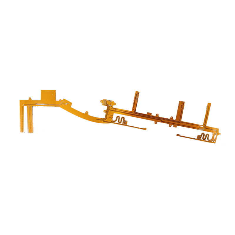
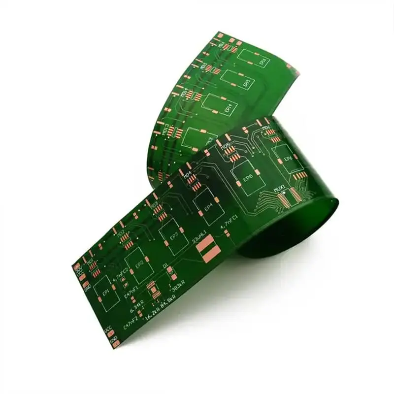
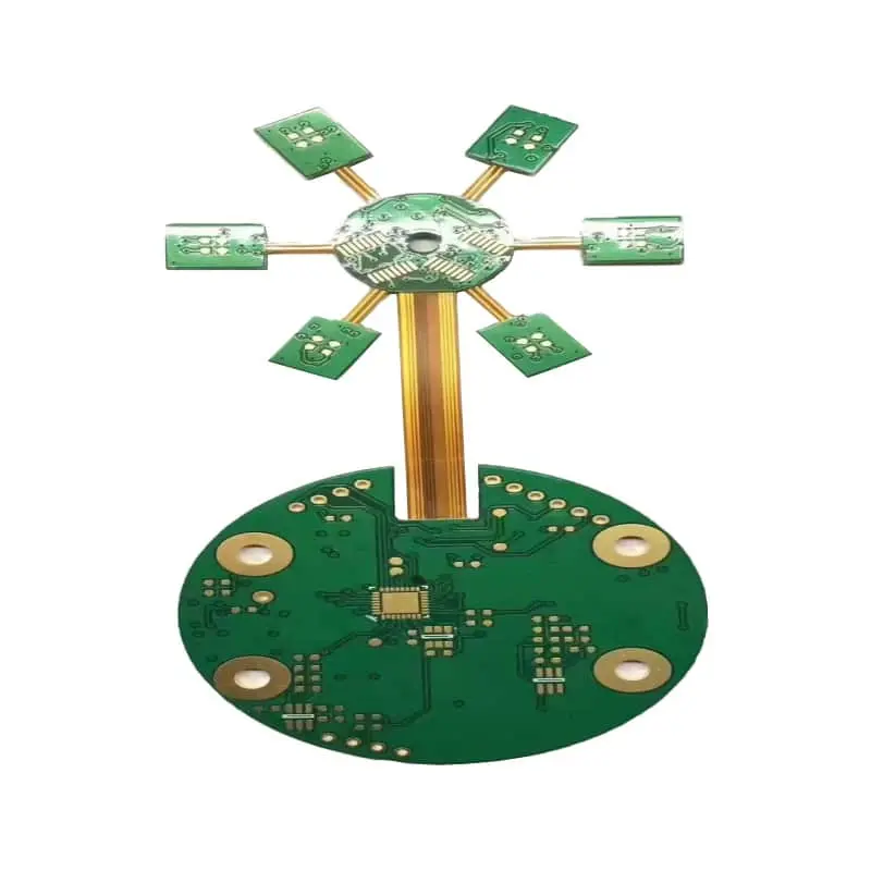
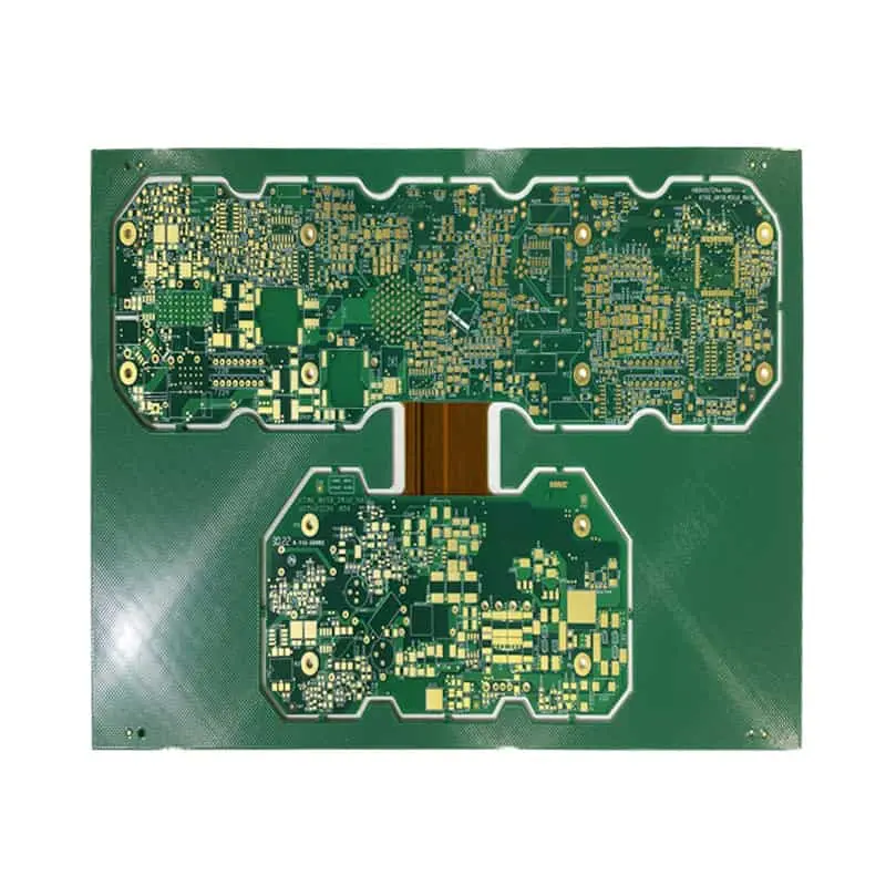
Match the construction to the application. Consumer electronics favors OSP or ENIG on standard FR-4. Automotive and medical boards usually require IPC Class 2–3 with tighter positional hole tolerances (±2 mil). Flex and rigid-flex suit compact medical, wearable, and camera-module designs but add 30–50% cost and 3–5 days of lead time; keep the bend radius at or above 10× the flex thickness and confirm the shop’s minimum flex layer count (typically 2–4 for rigid-flex).
Finally, run the supplier’s DFM checklist before ordering: annular ring, solder mask dams, aspect ratio, copper balance, and panelization. A 30-minute review routinely saves a full respin.
Quality, Testing, Certifications, and Compliance
For regulated products, quality paperwork matters as much as the board itself. Baseline requirements: ISO 9001 certification, UL recognition (the E-number should appear on your board), IPC-A-600 Class 2 or 3 workmanship, and RoHS/REACH compliance statements. Medical programs should add ISO 13485 and PPAP-level documentation; aerospace and defense programs may require ITAR registration, DFARS-compliant materials, and AS9100.
Match the test method to the risk. AOI catches pattern and solder-mask defects on every production board; flying-probe testing suits prototypes and small batches with no fixture cost; ICT is the fastest option at volume but requires test fixtures; and X-ray inspection verifies BGA solder joints, hidden vias, and internal layer registration. For high-reliability builds, add microsection analysis, ionic-contamination testing, and certificate-of-conformance lot traceability. A supplier should be able to explain which of these your product actually needs — over-testing burns budget, under-testing burns field reliability.
For compliance depth, ask for conflict-minerals declarations, material traceability down to the laminate lot, annual RoHS/REACH re-verification, and — for regulated sectors — anonymized case studies with first-pass yield and on-time delivery metrics. To protect your IP, confirm encrypted file transfer, signed NDAs, role-based access controls on Gerber and BOM data, and a documented data-retention policy.
Prototyping vs Volume Production: Workflows, Turnkey Assembly, and Project Management
Prototyping optimizes for speed and learning; production optimizes for cost and repeatability. Prototypes tolerate higher per-unit prices ($50–$500 per board), limited testing, and manual assembly. Volume builds demand validated processes, full test coverage, and consistent supply — but unit costs can fall 80–90% from prototype levels.
A disciplined NPI workflow bridges the two. Expect these milestones from a full-service supplier:
DFM review and quotation (2–3 days)
Engineering prototype build with a first-article inspection (FAI) report
Design validation and any respins
Pilot run (10–100 units) with process-capability data
Volume release with locked BOM, approved vendor list (AVL), and PPAP/FMEA documentation
Assign clear owners on both sides: a project manager for schedule, a quality engineer for FAI and test coverage, and a procurement lead for component strategy. Turnkey assembly — where the supplier sources components against your BOM and manages the AVL — reduces your workload but requires audit rights and a shortages-escalation clause.
Evaluate track record with data, not anecdotes: ask for on-time delivery percentage, first-pass yield by product family, and corrective-action history, plus relevant compliance case studies for regulated industries. Finally, agree on disruption playbooks up front: qualified second sources for critical laminates, buffer-stock agreements, and defined reroute options if a fab line goes down or a component is allocated.
Get a Quote in 24 Hours: What to Send Us
The fastest path to an accurate quote is a complete package:
Gerber or ODB++ files — all layers, including solder mask and silkscreen
BOM with manufacturer part numbers and approved alternates
Stackup drawing with controlled-impedance notes and special process requirements
Test requirements (ICT, flying probe, X-ray) and target quantity breaks
Contact our engineering sales team first for complex builds — an engineer reviewing your stackup on day one prevents expensive respins later. Use the quick-estimate form for instant budgetary pricing, or request a line-item quote with regional freight. Ask about free DFM feedback, sample boards before volume release, domestic quick-turn options, and current discounts on first orders and consolidated panel runs.
FAQ
How long do PCB manufacturing lead times typically take for prototypes and volume orders in the U.S., and what factors change those timelines?
Prototypes ship in 3–5 business days via quick-turn; volume orders take 2–4 weeks. Layer count, finish, test scope, materials, and shipping method all shift these windows.
What should a transparent, line-item PCB quote include so I can accurately compare suppliers?
Material, layer count, finish, drill/via charges, testing, assembly, packaging, freight, duties, and any NRE or expedite fees — with quantity breaks side by side.
What are common minimum order quantities for PCB fabrication and assembly, and how do they vary between prototype and mass production?
Prototypes start at 1–5 pieces, small batches at 10–50, and volume pricing typically begins at 100+ panels.
Which technical specs (minimum trace/space, layer count, drill sizes, via types) are most important to confirm before selecting a PCB supplier?
Trace/space, drill size and tolerance, layer count, blind/buried/via-in-pad support, and impedance control — matched to your stackup.
Which certifications and tests (IPC, ISO, UL, RoHS, X-ray, ICT) should I require for products in regulated sectors like medical or aerospace?
ISO 9001 as a baseline; ISO 13485 for medical; AS9100, ITAR, and DFARS for aerospace and defense; IPC Class 2/3 and UL throughout, plus X-ray for BGAs.
How do turnkey assembly and NPI workflows typically work with a full-service PCB supplier, and what project milestones should I expect?
DFM review, an FAI prototype, validation, a pilot run, then volume release with locked BOM/AVL and PPAP/FMEA documentation.
What specific measures should I ask a supplier to take to protect my IP and ensure secure handling of Gerber files and BOM data?
Encrypted transfer, signed NDAs, role-based access, documented retention policies, and ITAR-compliant data segregation for defense work.
About Author
David Chen https://www.linkedin.com/in/pcbcoming
David Chen is a Senior RF/PCB Process Engineer at Shenzhen Hongda Circuit Technology Co., Ltd., with over 12 years of experience in high-frequency PCB fabrication, impedance-controlled stack-up design, and Rogers/PTFE laminate processing. He also boasts an extensive professional background in PCBA manufacturing, PCBA testing, and PCBA optimization, with specialized expertise in high-precision PCBA fault analysis and rigorous PCBA reliability testing. The author has worked with high-layer-count server PCB fabrication, ultra-low-loss backplane stackups, and thermo-mechanical reliability optimization for AI infrastructure projects involving 112G and 224G PAM4 architectures. Skilled in complex circuit design and cutting-edge advanced PCB manufacturing processes, he delivers solutions that elevate product durability and performance across industrial applications. His technical articles focusing on PCBA manufacturing workflows and testing methodologies are widely cited by industry peers and technical platforms, and have gained attention and recognition from industry colleagues.