Turnkey PCB Assembly everything the standard articles don’t tell you — from counterfeit mitigation to test strategy economics, export compliance, and hidden cost structures.
Introduction
Most articles about turnkey PCB assembly cover the same ground: one vendor handles everything, you save time, quality improves. That framing is not wrong, but it is dangerously incomplete for engineers and procurement teams who are about to commit real money and real schedules to a contract manufacturer.
The gaps are not trivial. A misunderstood test strategy can cost you $30,000 in custom fixtures for a 50-unit prototype run. A single undetected counterfeit BGA can cascade into a product recall. An overlooked ITAR clause can trigger federal export violation proceedings. A poorly negotiated overage policy can leave you holding $15,000 in unused specialty components.
This guide addresses what the marketing brochures omit. It is written for the engineer who needs to evaluate a turnkey EMS partner critically, negotiate a contract intelligently, and anticipate failure modes before they appear on the production floor.
1. What Turnkey PCB Assembly Actually Means — A Precise Definition
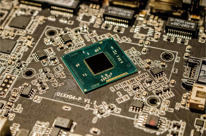
“Turnkey” derives from the concept of handing someone a key to a finished, immediately operational facility. In PCB assembly, it means the EMS (Electronics Manufacturing Services) provider assumes full responsibility for every step between receiving your design files and delivering tested, shippable assemblies.
A precise scope definition matters because “turnkey” is not a regulated term. Two vendors can both claim to offer turnkey services while delivering dramatically different scopes. Before signing anything, confirm exactly which of the following are included:
| Service Element | Often Assumed Included | Often Actually Excluded |
|---|---|---|
| DFM/DFA engineering review | ✓ | Detailed written report with corrective actions |
| Component sourcing | ✓ | Counterfeit verification, AVL management |
| PCB fabrication coordination | ✓ | Impedance validation, microsection reports |
| SMT assembly | ✓ | Nitrogen atmosphere reflow, void measurement |
| Through-hole assembly | ✓ | Selective soldering for mixed boards |
| AOI inspection | ✓ | 3D AOI with false-call rate SLA |
| Functional test | Often excluded | Test program development, fixture cost |
| Programming/flashing | Often excluded | Bootloader, calibration, serialization |
| Box build | Often excluded | Mechanical sub-assembly, labeling |
| Traceability documentation | Vague | Per-board component lot binding, IPC-1782 |
| RoHS Declaration of Conformity | Often excluded | Full DoC with supporting material certs |
Full turnkey means the EMS partner owns the supply chain from component sourcing to final delivery. Partial turnkey (consigned or hybrid) means the customer supplies some or all components while the EMS handles assembly and test. The right model depends on your organization’s supply chain maturity, your inventory position, and whether you have preferred or sole-source components that cannot be delegated to a third party.
2. Counterfeit Component Detection: The Risk Nobody Talks About Plainly
The global market for counterfeit electronic components is estimated in the billions of dollars annually. The aerospace, defense, and medical sectors see the highest exposure, but commercial electronics are not immune. A counterfeit IC is not merely a non-functional part — it is a part that may pass initial electrical screening while failing under thermal stress, vibration, or after 500 hours of operation.
Why Turnkey Amplifies the Risk — and the Opportunity
When your EMS partner sources components, you lose direct visibility into the supply chain. This is the double-edged nature of turnkey: you gain efficiency but surrender control. The question is not whether to delegate sourcing — it is how to verify that your EMS partner’s counterfeit mitigation practices are substantive, not cosmetic.
What Genuine Counterfeit Mitigation Looks Like
Authorized distribution hierarchy. A rigorous EMS will maintain a tiered sourcing policy:
- Direct from manufacturer (e.g., TI, NXP, STMicroelectronics)
- Franchised authorized distributors (Digi-Key, Mouser, Arrow, Avnet, Future Electronics)
- Independent distributors with full traceability documentation
- Open market / broker channels — only with explicit customer approval and enhanced inspection
Parts from tiers 3 and 4 should trigger mandatory physical and electrical verification regardless of documentation claims.
Physical inspection protocols per IDEA-STD-1010 and SAE AS6081. Ask your EMS partner specifically which of the following they perform:
- Visual inspection under 10x–40x magnification: Checks for remarking, sanding marks (surface re-labeling to change part numbers or date codes), mold parting line inconsistencies, and lead finish anomalies.
- XRF (X-Ray Fluorescence) spectroscopy: Verifies lead finish composition (HASL vs. ENIG vs. matte tin) and detects lead-free parts relabeled as leaded — a common fraud that causes field failures when mixed alloy soldering produces brittle tin-bismuth joints.
- X-Ray inspection (radiography): Reveals internal die size, bond wire patterns, and voiding inconsistencies that indicate die harvesting from non-conforming parts.
- Decapping and die verification: For high-value or safety-critical components, chemical or laser decapping exposes the die for comparison against authenticated die markings. This is rare in commercial production but standard in aerospace procurement.
- Electrical parametric testing: Beyond go/no-go functional tests, parametric screening verifies that leakage currents, threshold voltages, and timing parameters match the datasheet — rejecting parts that are functional but out-of-spec.
MSL (Moisture Sensitivity Level) compliance. This is a frequently overlooked risk. Components rated MSL 3 or higher must be stored in dry conditions (typically <10% RH) and baked before reflow if the floor life has been exceeded. An EMS partner handling consigned components should document the floor life status of every moisture-sensitive part. A single batch of out-of-condition components going through reflow can cause internal delamination (“popcorning”) — producing boards that pass all post-assembly electrical tests but fail prematurely in the field.
Red Flags When Evaluating an EMS Partner’s Counterfeit Program
- They cannot name their primary distribution agreements
- They offer dramatically below-market pricing on long-lead or allocated components without explanation
- Their counterfeit mitigation policy is a single paragraph in a quality manual
- They have no documented procedure for handling suspected counterfeit finds
- They cannot provide Certificate of Conformance (CoC) and lot traceability for every line item on your BOM
3. NPI Engineering: What Actually Happens Before the First Board Is Built
New Product Introduction (NPI) is the engineering-intensive phase between design handoff and first production build. In turnkey assembly, this phase is where the most value is created — and where the most costly mistakes are prevented. Yet most articles treat it as a checkbox: “DFM review included.”
The reality is that a thorough NPI process involves hundreds of discrete engineering decisions. Here is what a competent EMS partner’s NPI team should deliver.
DFM (Design for Manufacturability) Review — Specific Checkpoints
A meaningful DFM review is not a software scan against a generic rule set. It is an engineer reading your specific design against your specific manufacturing process window. Critical checks include:
Pad geometry and solder paste aperture design:
- IPC-7351 footprint compliance for all SMD components
- Solder mask defined (SMD) vs. non-solder-mask-defined (NSMD) pad selection for BGAs — NSMD pads are generally preferred for improved solder joint reliability
- Paste aperture area ratio: the ratio of aperture area to aperture wall area should be ≥0.66 to ensure consistent paste release from the stencil. Violations here cause insufficient solder volume and tombstoning on 0201 and 01005 components
- Stencil thickness selection (typically 100–150 μm) balanced against the smallest component pitch on the board
Component placement and process flow:
- Minimum component-to-component spacing per IPC-7351 (e.g., 0.15 mm for 0402 to 0402, larger for connectors and through-hole near SMD)
- Component orientation relative to reflow direction — capacitors and resistors should be oriented perpendicular to the reflow conveyor direction to equalize thermal mass and prevent tombstoning
- Keepout zones around connectors, test points, and fiducial marks
- Via-in-pad detection: vias under BGA pads must be filled (non-conductive epoxy fill + planarization) to prevent solder wicking during reflow
Testability (DFT — Design for Test):
- Test point coverage ratio: a well-designed board provides test access to ≥80% of nets
- Test point minimum size (typically 1.0 mm diameter for bed-of-nails ICT, 0.5 mm for flying probe)
- Test point grid compliance (2.54 mm or 1.27 mm grid preferred for ICT fixture compatibility)
- JTAG/Boundary Scan chain integrity — discussed further in Section 5
Thermal relief and copper pour design:
- Thermal relief spoke design on through-hole pads embedded in copper pours — insufficient relief causes cold joints due to heat sinking during wave or selective soldering
- Copper balance across layers — asymmetric copper distribution causes bow and twist, critical for fine-pitch BGAs
DFA (Design for Assembly) Review — Beyond Component Spacing
DFA extends beyond clearances to consider the physical reality of your assembly process:
- Pick-and-place compatibility: Components must have a flat, vacuum-pickable surface. Parts in non-standard orientations (e.g., connectors placed horizontally) may require custom nozzles or manual placement, adding cost and reducing yield.
- Polarity and orientation marking: Every polarized component (capacitors, diodes, ICs) must have unambiguous polarity indication visible after placement. This is a design issue, not just a manufacturing issue.
- Conformal coating masking: If conformal coating is required, the design must include adequate clearance around masked areas (connectors, test points, programming headers), and the mask design must be provided to the EMS as a separate layer.
First Article Inspection (FAI)
The First Article Inspection is the formal verification event at the end of NPI. Before any production quantity is built, the EMS team and customer engineering jointly verify that:
- All components are correct part numbers, correct orientation, and correctly placed
- Solder joint quality meets IPC-A-610 Class 2 or Class 3 criteria
- Board dimensions and mechanical features meet drawing requirements
- Functional test passes all defined test cases
- All serialization, labeling, and marking requirements are satisfied
The FAI report becomes a controlled document. Any subsequent change — a component substitution, a process parameter adjustment, a layout revision — requires a formal Engineering Change Order (ECO) and may trigger a partial or full re-FAI depending on the scope of the change.
ECO Management During Prototype Iterations
Hardware development rarely proceeds without design changes. A competent turnkey partner has a structured ECO process that includes:
- Documented change request with engineering justification
- Impact assessment: which boards in inventory or in-process are affected
- Disposition of non-conforming material (rework vs. scrap vs. use-as-is with deviation)
- Updated BOM and assembly drawing revision control
- Clear communication of change-driven cost and schedule impact before execution
The absence of formal ECO management is one of the most reliable indicators of an EMS partner that will create problems at scale.
4. Supply Chain Risk Management: Long Lead Times, EOL Parts, and the Allocation Crisis
The component shortage cycles of 2020–2022 exposed a fundamental vulnerability in electronics supply chains that most OEMs had underestimated. A turnkey EMS partner’s supply chain capabilities are not a commodity — they are a strategic differentiator.
Component Lifecycle Monitoring
Every component on your BOM has a lifecycle status. The standard classifications are:
- Active: In production, full availability
- NRND (Not Recommended for New Designs): Manufacturer is signaling intent to discontinue; still available but end of life is approaching
- EOL (End of Life): Last-time buy window is open or has passed
- Discontinued/Obsolete: No longer manufactured
A competent EMS partner monitors lifecycle status continuously for every component in active production programs. When a part transitions to NRND, they should proactively notify the customer and present options: last time buy (LTB) quantity calculation, equivalent alternative part identification, or design revision recommendation.
Last Time Buy (LTB) strategy: Calculating the optimal LTB quantity requires estimating the remaining product life, the cost of redesigning around a replacement part, and the carrying cost of holding excess inventory. Most customers systematically underestimate LTB quantities because they underestimate remaining product life.
Approved Vendor List (AVL) Management
For every critical component, a mature EMS maintains an AVL — a pre-qualified list of acceptable manufacturers and their authorized distribution channels. When a primary source becomes unavailable (allocation, price spike, quality issue), the EMS can immediately pivot to a pre-qualified alternative without delaying production.
AVL management includes:
- Qualification testing for alternate sources (electrical parametric testing, reliability testing)
- Formal approval process requiring customer sign-off for changes to safety-critical parts
- Conflict minerals compliance tracking per Dodd-Frank Section 1502
Managing 52-Week Lead Time Components
Some components — particularly FPGAs, high-performance microprocessors, certain power management ICs, and specialized RF components — regularly carry lead times of 40–60 weeks from authorized sources. In a turnkey program, this means:
- BOM lead time analysis must be performed immediately upon design freeze, not when the purchase order is placed
- The EMS partner should offer component pre-ordering as a service — purchasing long-lead items against a purchase commitment before the full production order is confirmed
- Staggered delivery schedules can be negotiated: short-lead components are ordered normally while long-lead items are ordered immediately
An EMS partner who waits for your purchase order before analyzing BOM lead times is not a supply chain partner — they are an order processor.
5. Test Strategy: The Economics and Engineering of Getting It Right
Testing is the most technically nuanced and commercially consequential decision in PCB assembly. It is also the area where engineers most frequently accept a vendor’s default offering without understanding what they are — and are not — getting.
The Five Primary Test Methods and When to Use Each
1. Automated Optical Inspection (AOI)
AOI uses structured light and cameras to detect visual defects: missing components, wrong polarity, solder bridges, insufficient solder, tombstoning. Modern 3D AOI systems measure solder joint height and volume, not just 2D appearance.
AOI is fast, non-destructive, and standard in virtually all SMT production lines. However, it cannot detect:
- Electrically open joints that are visually correct (head-in-pillow defect on BGAs)
- Incorrect component values (a 100Ω resistor looks identical to a 1kΩ)
- Functional failures
When to use: Always. AOI is table stakes for any professional SMT line.
2. X-Ray Inspection (AXI/3D X-Ray)
X-ray inspection reveals solder joint quality beneath components that are visually inaccessible: BGAs, QFNs, LGAs, and bottom-terminated components. 3D CT X-ray (computed tomography) allows cross-sectional slice imaging to detect voids within individual solder balls.
The IPC-7095D standard defines acceptable void percentages: typically ≤25% void area per joint for Class 2, with tighter limits for Class 3 thermal/RF applications. Excessive voiding increases thermal resistance and reduces joint fatigue life.
When to use: Any board with BGAs, QFNs, or other bottom-terminated packages. Also critical for high-power boards where thermal performance depends on low-void die-attach connections.
3. In-Circuit Test (ICT) / Bed-of-Nails
ICT uses a custom spring-probe fixture (“bed of nails”) to contact test points on the assembled board. It verifies component presence, value, orientation, and basic circuit connectivity. ICT can test resistors, capacitors, inductors, diodes, and transistors parametrically.
The economic reality of ICT: Fixtures cost $5,000–$30,000 depending on board complexity and pin count. This cost is amortized over the production run. For a 100-unit prototype run, an $8,000 fixture adds $80 per board in NRE — which is often unacceptable. For a 10,000-unit production run, the same fixture adds $0.80 per board.
ICT is the right choice when: production volumes justify fixture amortization, board complexity makes manual inspection impractical, and test point coverage is adequate (>80% net coverage).
4. Flying Probe Test
Flying probe uses 2–8 motorized probes that move to programmed coordinates on the board to make electrical measurements without a custom fixture. Programming takes 4–8 hours versus 4–8 weeks for ICT fixture fabrication.
Flying probe is slower than ICT (5–30 minutes per board versus 30–120 seconds) and has lower test coverage for dense designs, but has zero fixture cost.
When to use: Prototypes, NPI builds, low-volume production (typically <500 units), boards with frequent design revisions that would require expensive fixture modifications.
5. Functional Test (FCT)
Functional test powers up the fully assembled board and exercises it against a defined test specification. Unlike ICT (which tests component-level properties), FCT tests system-level behavior: firmware execution, I/O verification, communication interface validation, power consumption measurement.
The critical question nobody asks: Who develops the functional test program? This is almost never included in standard turnkey pricing. Test program development is an engineering effort that can range from 20 engineering hours for a simple sensor board to 200+ hours for a complex multi-core processor board. This cost belongs in your project budget, and the responsibility for test specification must be defined contractually before NPI begins.
FCT fixture design (interface connectors, power supply margins, signal conditioning) adds additional NRE cost. The customer’s engineering team typically owns the test specification; the EMS partner typically builds the fixture and executes the test.
Programming, Serialization, and Calibration
For any board with programmable devices — microcontrollers, FPGAs, DSPs, EEPROMs — the assembly process must include:
- Firmware programming: The EMS needs the final firmware binary, a validated programming tool (JTAG programmer, SPI flash programmer, proprietary bootloader), and a defined programming procedure. Version control is critical: which firmware version is released for which production lot?
- Serialization: Many products require unique serial numbers flashed into non-volatile memory at production time. The EMS must be capable of managing a serial number database and providing traceability between physical board serial numbers and production records.
- Factory calibration: Sensor-based products often require individual calibration against a known reference at end-of-line. The calibration coefficients are typically stored in the device’s non-volatile memory. The calibration process requires a test station, reference instruments with traceable calibration, and a defined pass/fail criterion.
None of these capabilities should be assumed. Confirm them explicitly during EMS partner qualification.
Selecting the Right Test Strategy: A Decision Framework
| Scenario | Recommended Strategy |
|---|---|
| Prototype (<25 units) | Flying probe + functional test (if FCT program exists) |
| NPI build (25–200 units) | Flying probe + FCT + X-ray for BGAs |
| Low-volume production (200–2,000 units) | Evaluate ICT fixture ROI; flying probe if negative |
| High-volume production (>5,000 units) | ICT + AOI + X-ray + FCT |
| Safety-critical (medical, aerospace) | Full test battery + burn-in/HALT regardless of volume |
6. Thermal Design and Process Reliability: What Happens Inside the Oven
The reflow soldering process is a tightly controlled thermal event. Getting it wrong produces defects that may not be immediately visible or electrically detectable but that compromise long-term reliability. A professional EMS partner treats oven profiling as an engineering activity, not an operator judgment call.
Reflow Profile Engineering
A reflow profile defines oven temperature as a function of time for the board traveling through the conveyor oven. The profile has four zones:
- Preheat zone: Ramp rate typically 1–3°C/second. Too fast causes thermal shock; too slow activates flux prematurely.
- Soak zone: Holds at 150–180°C for 60–120 seconds. Activates flux, equalizes board temperature, burns off solvent.
- Reflow zone (liquidus): Peak temperature 235–250°C for SAC305 lead-free alloy. Time above liquidus (TAL) typically 45–75 seconds. Too short produces insufficient intermetallic formation; too long causes excessive intermetallic growth (brittle joints) and component thermal damage.
- Cooling zone: Controlled cooling rate affects grain structure of the solder joint. Faster cooling (within limits) produces finer grain structure and better fatigue resistance.
Profile validation should use actual thermocouples attached to representative locations on the production board — not a generic profile from a previous job. Heavy copper pours, large heat-sinking connectors, and fine-pitch BGA components all create thermal gradients that must be characterized.
Lead-Free and Mixed Alloy Considerations
The industry transition to lead-free solder (driven by RoHS directive) introduced a practical complication: some components — particularly military-specification parts, certain high-reliability passive components, and parts from older inventory — are only available with SnPb (tin-lead) terminations. When these are assembled onto a board using SAC305 paste, you have a mixed alloy joint.
Mixed alloy joints can form tin-bismuth or other intermetallic phases with different mechanical properties than either pure alloy. The reliability implications depend on the alloy combination, the joint geometry, and the service environment. For commercial applications, mixed alloy is often acceptable with appropriate engineering review. For aerospace and defense applications, formal mixed alloy qualification testing is typically required.
7. Traceability Documentation: What “Full Traceability” Should Actually Mean
The word “traceability” appears in virtually every EMS marketing document. In practice, traceability ranges from “we keep purchase orders on file” to genuine cradle-to-grave component-level documentation. For regulated industries (medical devices per FDA 21 CFR Part 820, aerospace per AS9100, automotive per IATF 16949), the standard is unambiguous. For commercial electronics, it is a negotiated specification.
The IPC-1782 Standard for Traceability
IPC-1782 defines four traceability levels:
- Level A: Batch-level traceability. Components are tracked to their purchase order and manufacturer lot code, but not to individual boards.
- Level B: Board-level traceability. Each assembled board has a unique identifier, and the component lots used to build it are recorded.
- Level C: Component-level traceability. Each individual component instance on each board is tracked — which specific reel was used for position R42 on board serial number 00147.
- Level D: Process-level traceability. In addition to component tracking, machine settings, operator IDs, environmental conditions, and inspection results are recorded for each board.
Most commercial turnkey programs operate at Level A or B. Medical and aerospace programs typically require Level C or D.
What a Proper Delivery Data Package Should Contain
When your boards are delivered, the following documentation should accompany them:
- Assembly travelers (build records for each board lot)
- SPI (Solder Paste Inspection) reports — paste volume and area measurements for each board
- AOI reports — pass/fail results and image captures for any flagged defects
- X-ray reports — void percentage measurements for all BGA/QFN joints
- ICT/Flying probe reports — test results and any anomalies
- FCT reports — functional test results with pass/fail status and any measured parameters
- Component Certificate of Conformance (CoC) — from each component supplier
- RoHS Declaration of Conformity — signed statement of RoHS compliance with supporting material certifications
- Serialization records — mapping of board serial numbers to component lot numbers and test results
If your EMS partner cannot provide this package upon request, you have a liability exposure that will surface during a product audit, a field failure investigation, or a regulatory inspection.
8. The Real Cost Structure of Turnkey PCB Assembly
Standard turnkey quotes present a per-unit price that obscures the full cost structure. Understanding the complete economics prevents budget surprises and enables more accurate product costing.
NRE (Non-Recurring Engineering) Costs
NRE costs are one-time engineering investments that are not reflected in the per-unit price:
| NRE Item | Typical Cost Range | Notes |
|---|---|---|
| SMT stencil (laser-cut stainless) | $150–$400 per stencil | One stencil per board side; nano-coated stencils add ~$50 |
| ICT fixture | $5,000–$30,000 | Depends on pin count, board size, complexity |
| Functional test fixture | $2,000–$15,000 | Hardware only; software is separate |
| FCT software development | $5,000–$50,000 | Engineering hours; customer typically responsible |
| BGA X-ray program setup | $200–$800 | Per board type |
| Custom programming fixture | $500–$3,000 | If standard JTAG/SWD is insufficient |
Component Overage and Shortage Policies
Surface mount component placement involves inherent material losses: failed pick-and-place attempts (component thrown by the machine), inspection rejects, and setup calibration waste. Standard industry allowance is 2–5% overage depending on component size (smaller components have higher loss rates).
For prototype builds, EMS partners typically require you to supply or pay for a flat overage quantity (e.g., 10 extra units per line item for 0402 passives, 3 extra units for ICs). Clarify this policy before finalizing your BOM pricing.
What happens to excess components? This is a contractual matter that is frequently ambiguous:
- Customer-owned consigned components: excess should be returned or held in bonded storage
- EMS-sourced turnkey components: excess may be retained by the EMS or charged back to the customer depending on minimum order quantities
Minimum order quantities (MOQ) are the other hidden cost. If a line item requires 100 units but the distributor MOQ is 1,000, you are paying for 900 units you will not use. A competent EMS partner will flag MOQ issues during BOM scrub and either find alternative sources with lower MOQ or build the excess cost into their quote transparently.
Change Order (ECO) Cost Impact
Each engineering change during prototype iterations carries cost implications:
- BOM change (component substitution): May require restocking fees, expedited procurement, re-inspection
- Gerber change (layout revision): New stencil required ($150–$400), possible fixture modification
- Process change: Re-profiling, re-programming, re-qualification
Establishing a clear ECO pricing framework in your master service agreement (MSA) before NPI begins prevents adversarial negotiations during the time-pressured prototype phase.
9. Export Control and Trade Compliance: The Risk Most OEMs Ignore
Export control regulations represent one of the highest-consequence compliance risks in electronics manufacturing — and one of the least discussed in vendor selection conversations.
ITAR (International Traffic in Arms Regulations)
ITAR controls the export, import, and domestic transfer of defense articles and services. PCB assemblies that are designed for or incorporated into defense applications may be ITAR-controlled even if the individual components are commercially available.
For OEMs, the key implications in a turnkey program are:
- Technical data transfer: Gerber files, assembly drawings, and BOM for ITAR-controlled articles cannot be shared with foreign persons — including employees of your EMS partner who are not U.S. persons — without a license or applicable exemption
- Manufacturing location: ITAR-controlled assemblies typically must be manufactured in the United States by U.S.-person employees
- Subcontracting: Your EMS partner cannot subcontract ITAR work to a foreign facility without separate authorization
Several of the providers referenced in publicly available turnkey assembly content explicitly state they do not process ITAR orders in their online services. This is the correct policy; the problem is that many OEMs do not know whether their product is ITAR-controlled.
EAR (Export Administration Regulations)
EAR controls the export of dual-use items — commercial technologies that have potential military applications. Many high-performance semiconductor devices (advanced FPGAs, encryption-capable processors, certain RF components) carry Export Control Classification Numbers (ECCNs) that require export licenses for certain destinations.
In a turnkey program, if your EMS partner is sourcing components on your behalf, they need to know the ECCN status of controlled parts to ensure compliant export documentation when the finished assemblies are shipped internationally.
Country of Origin and Supply Chain Transparency
U.S. Customs and Border Protection applies tariffs and duty rates based on the country of origin of finished goods. For PCB assemblies, the country of origin is generally determined by the country where “substantial transformation” occurred — typically where the components were soldered to the board.
Assemblies manufactured in China may be subject to Section 301 tariffs (25% on many electronics categories) when imported into the United States. This has driven a significant shift toward assembling in countries not subject to these tariffs: Mexico, Southeast Asia (Vietnam, Thailand, Malaysia), or domestic U.S. manufacturing.
A competent turnkey partner will provide Certificate of Origin documentation and advise on supply chain structuring to optimize duty exposure — this is not tax advice, but it is legitimate supply chain planning.
10. Evaluating and Qualifying an EMS Partner: A Practical Framework
With the technical context established, here is a structured approach to EMS partner qualification that goes beyond the standard “send us your ISO certificate” checklist.
Technical Qualification Questions
On counterfeit mitigation:
“Walk me through your procedure when a component arrives from an independent distributor. What physical inspections do you perform, and where are those procedures documented in your quality system?”
On test strategy:
“For a board with three BGAs and a 32-bit processor, what test coverage would your standard AOI + flying probe offer? What would you recommend to achieve >90% fault detection coverage, and what would that cost?”
On NPI process:
“Show me the DFM report format you provide at the end of engineering review. What’s your typical defect detection rate on NPI builds versus first production builds?”
On supply chain:
“How do you monitor component lifecycle status for active programs? Give me an example of an EOL situation you proactively caught and how you handled it.”
On traceability:
“What is the highest traceability level (per IPC-1782) that your MES system supports? Can you demonstrate a sample delivery data package?”
Process Audit Checklist
When visiting or auditing an EMS facility:
- Observe the incoming inspection process for a recently received component shipment
- Review the solder paste management log (paste age, temperature storage, refrigerator log)
- Verify reflow profile documentation for an active production board
- Review the most recent internal audit findings and corrective actions
- Examine a sample board traveler from a completed production lot
- Verify calibration certificates for critical measurement equipment (AOI, X-ray, reflow profiler)
- Confirm ESD compliance (flooring, wrist straps, workstation grounding)
Frequently Asked Questions
Q1: My component has a 52-week lead time and I need boards in 16 weeks. What are my options in a turnkey program?
A: There are four practical paths. First, ask your EMS partner to check broker inventory immediately — authorized brokers sometimes carry allocation stock at premium, and for small quantities (prototype builds), this premium may be acceptable. Second, investigate pin-compatible alternate sources; your EMS partner’s AVL team can often identify a drop-in replacement with shorter lead time, but this requires formal qualification if the part is in a safety-critical circuit. Third, consider a partial build: order all other components and manufacture the PCBs now, leaving the long-lead components unpopulated. When the parts arrive, the boards go through a second pass. This adds assembly cost but preserves schedule for the rest of the bill of materials. Fourth, if the long-lead component is in the critical path of your product launch, seriously evaluate whether a design change to an available alternative is faster than waiting. A one-week redesign plus a four-week build cycle beats a 52-week wait.
Q2: How do I know if I actually need ICT versus flying probe? My EMS partner keeps recommending ICT for everything.
A: The decision is an economic calculation, not a technical absolute. ICT is faster and provides higher fault coverage on dense boards, but the fixture is a fixed cost that only makes sense when amortized over sufficient volume. The break-even quantity is approximately: fixture cost ÷ (ICT test cost per board savings vs. flying probe). For a $10,000 fixture and a $15/board test time difference, break-even is approximately 667 boards. Below that quantity, flying probe is more economical. Additionally, if your design is still changing (as it typically is during NPI), an ICT fixture becomes obsolete with every board revision requiring probe point changes — a costly and time-consuming process. Use flying probe for all prototype and NPI builds, and re-evaluate ICT only when you have a production-frozen design and a confirmed volume forecast that justifies the fixture investment.
Q3: What exactly is “head-in-pillow” defect in BGA assemblies, and can my vendor’s standard AOI catch it?
A: Head-in-pillow (HIP) is a BGA solder joint defect where the solder ball from the component and the solder paste on the PCB pad each melt independently but fail to coalesce into a unified joint. The result looks like a perfect solder ball sitting in a pillow of separate solder — hence the name. The joint has mechanical contact but no reliable electrical or metallurgical bond. HIP defects are insidious because they often pass initial electrical test but fail intermittently under thermal cycling or mechanical stress, causing hard-to-reproduce field failures. Standard 2D AOI cannot detect HIP because it only images the visible top surface of the board. Even 3D AOI has limited detection capability for HIP. The only reliable detection method is 3D X-ray inspection, which reveals the characteristic double-dome shape (two separate solder hemispheres rather than one merged joint). If your design includes BGAs, X-ray inspection is not optional — it is the minimum responsible standard of care.
Q4: My product will be sold in Europe and the US. What documentation does my EMS partner need to provide for RoHS compliance, and what’s the difference between RoHS 2 and the original RoHS directive?
A: The original RoHS directive (2002/95/EC) restricted six substances in electrical and electronic equipment: lead, mercury, cadmium, hexavalent chromium, PBB, and PBDE. RoHS 2 (2011/65/EU, later amended by 2015/863/EU) added four additional restricted substances: DEHP, BBP, DBP, and DIBP (phthalates), and extended scope to cover additional product categories including industrial equipment and medical devices. For your EMS partner, the documentation requirement is a material Declaration of Conformity (DoC) that: identifies the specific substances restricted, confirms the product meets the concentration thresholds (typically 0.1% by weight per homogeneous material, 0.01% for cadmium), and provides supporting material safety data sheets (MSDS/SDS) or IPC-1752A material declarations from component suppliers for every line item on the BOM. Ask your EMS partner specifically whether their DoC is based on actual material declarations from suppliers or on generic assumptions. Generic assumptions are legally insufficient for regulated products including medical devices.
Q5: I’m considering splitting my program between a domestic US EMS for prototypes and a lower-cost overseas EMS for production. What are the hidden costs and risks of this handoff?
A: This is a common strategy and a frequent source of expensive surprises. The transition risks fall into four categories. First, process equivalence: the overseas facility runs different equipment, different solder alloys, different stencil designs, and different inspection thresholds than the domestic prototype house. What passed at the domestic facility may not pass at the overseas facility — or vice versa. Establishing process equivalence requires a formal qualification build at the production facility, not just a paper review. Second, documentation transfer: the domestic EMS holds your process traveler, reflow profile, inspection programs, and test programs. These must all be transferred, validated, and potentially rebuilt for different equipment — this is an engineering effort, not an administrative one. Third, counterfeit risk at scale: overseas manufacturing at high volume through broker channels dramatically increases counterfeit exposure. Your overseas EMS partner’s counterfeit mitigation practices must be audited, not assumed. Fourth, communication and iteration latency: during early production, design issues inevitably surface. Resolving them across a 12-hour time zone difference with language barriers adds days to each iteration cycle. The true cost of the overseas handoff must include the engineering cost of the transition, the first-article qualification build, travel for on-site audit, and the risk reserve for first-production yield losses.
Q6: My board has components that require programming after assembly. How should this be structured in a turnkey program, and who owns the test program?
A: Programming responsibility is one of the most frequently ambiguous elements of a turnkey contract. The clean answer is: the customer owns the firmware and the test specification; the EMS partner owns the execution infrastructure. Specifically, your engineering team should provide the EMS with: the firmware binary (versioned and signed with an MD5/SHA hash for integrity verification), a documented programming procedure (tool, interface, voltage, speed settings), a verification step that confirms successful programming (typically a readback and compare, or a simple boot verification), and pass/fail criteria. The EMS is responsible for: procuring or building the programming fixture (JTAG adapter, pogo-pin board, or proprietary interface), integrating programming into the assembly flow at the correct process step (pre-reflow for some device types, end-of-line for others), maintaining a programming log that records the firmware version, batch number, and programming timestamp for each board serial number, and managing firmware version updates when you release new firmware to production. Critical: establish a formal firmware release process. The EMS should never accept firmware updates via informal email attachments. Use a controlled release mechanism — even a simple shared document with version numbers and hash values — to ensure that the right firmware version goes onto the right boards.
This article was written to address the technical gaps commonly found in commercially available turnkey PCB assembly guides. The intent is to equip engineers and procurement teams with the specific knowledge needed to select, qualify, and manage an EMS partner effectively.
About Author
David Chen https://www.linkedin.com/in/pcbcoming/
David Chen boasts an extensive professional background in PCBA manufacturing, PCBA testing, and PCBA optimization, with specialized expertise in high-precision PCBA fault analysis and rigorous PCBA reliability testing. Skilled in complex circuit design and cutting-edge advanced PCB manufacturing processes, he delivers solutions that elevate product durability and performance across industrial applications. His technical articles focusing on PCBA manufacturing workflows and testing methodologies are widely cited by industry peers, research institutions, and technical platforms, solidifying his reputation as a recognized technical authority in the global circuit board manufacturing sector.