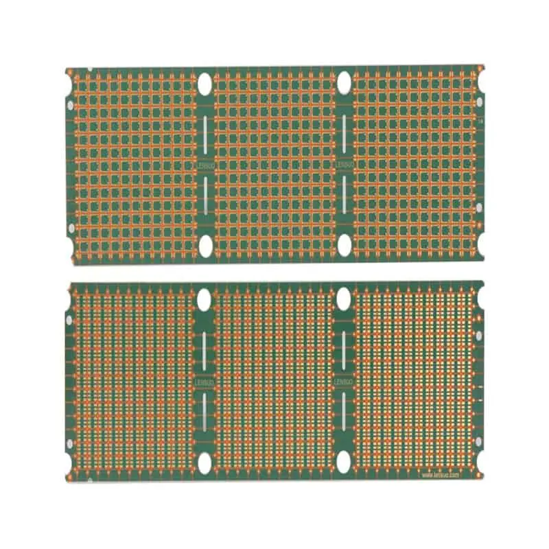
Custom PCB service
Custom PCB service is a professional manufacturing solution that designs and builds printed circuit boards from scratch based on your product’s electrical performance, mechanical structure, operating environment, and mass production needs. Unlike standard off-the-shelf PCBs, it delivers fully tailored boards for high-end electronics requiring high speed, high frequency, high density, high reliability, and high power handling.
Custom PCB Manufacturing: HAODA ELECTRONIC CO., LIMITED
In today’s fast-growing electronics industry, custom PCB manufacturing is a core driver of innovation, widely used in AI servers, 5G communications, medical wearables, automotive electronics, and more. As a leading provider of precision circuit board solutions, HAODA ELECTRONIC CO., LIMITED has long focused on turning cutting-edge design ideas into high-performance, highly reliable PCBs. In 2026, we integrate the industry’s latest breakthrough technologies into our custom manufacturing services, delivering world-class quality, ultra-high precision, and scalable delivery to customers worldwide.
The Core of Custom PCB Manufacturing: Tailored Solutions for Unique Design Needs
Custom PCB manufacturing goes far beyond standard board production. It’s a customer-centric, end-to-end process built around your specific electrical, mechanical, and reliability requirements. At HAODA ELECTRONIC CO., LIMITED, we know no two projects are the same: a high-frequency RF board for 6G infrastructure is nothing like a rigid-flex board for medical wearables; a high-layer backplane for AI servers is completely different from a high-density interconnect (HDI) board for consumer electronics.
Our full-range custom options include:
- Material selection: From traditional FR4 to 2026’s ultra-low-loss high-frequency materials (M9/M10 series, HVLP copper foil substrates)
- Layer count: 1–78 layers, supporting 7-level HDI and any-layer interconnect / stacked vias
- Precision specs: Line width / spacing down to 2.5/2.5 mils, laser microvias as small as 0.075 mm
- Special functions: 6–10 oz+ heavy copper for EV powertrains, embedded thermal management, integrated rigid-flex structures
- Surface finishes: ENIG, OSP, immersion tin, and custom solder mask colors to fit assembly and environmental needs
Every project starts with rigorous DFM (Design for Manufacturability) review. Our engineering team optimizes your design to improve producibility, cost efficiency, and performance, lower risks, and speed up time to market.
Latest PCB Manufacturing Technologies Integrated into Custom Services in 2026
2026 marks a major turning point for the PCB industry. The AI boom, high-speed communications (800G / 1.6T optical modules), and miniaturization trends are reshaping the sector. HAODA ELECTRONIC CO., LIMITED has heavily upgraded its production lines with these game-changing technologies to keep our custom PCB services at the industry forefront.
1. Ultra-Low-Loss High-Frequency Materials (M9/M10 & HVLP Copper Foil)
2026 is the year of mass adoption for M9 materials, officially specified by NVIDIA’s Rubin architecture for next-gen AI platforms. We’re also advancing M10 material testing, targeting a 30–40% lower signal loss than traditional FR4 — critical for 800G / 1.6T optical modules and high-performance computing (HPC) systems.
HAODA ELECTRONIC CO., LIMITED is among China’s first manufacturers to mass-produce M9/M10 substrates and HVLP (very low profile) copper foil. Our HVLP5 copper foil (surface roughness < 1.5 μm) minimizes signal attenuation at speeds above 224Gbps. Low-Dk Q-glass cloth cuts dielectric loss by 30% vs. standard E-glass cloth. This technology powers AI servers, 5G/6G base stations, and high-speed data center backplanes.
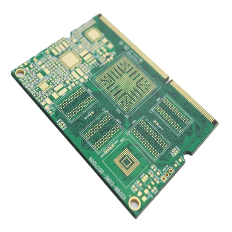
2. Advanced HDI & Any-Layer Interconnect Technology
In 2026, consumer and medical electronics demand strict miniaturization and high-density packaging. Our custom service supports 7-level HDI and any-layer interconnect, with laser microvias at 0.075 mm and stacked vias enabling BGA fanout at 0.4 mm pitch and below.
We use Direct Laser Imaging (DLI) for fine line production, achieving line width / spacing precision of ±0.1 mil — 30% more accurate than traditional exposure. This technology is essential for smart glasses, wearables, IoT sensors, and other compact devices, preserving signal integrity in space-constrained designs.
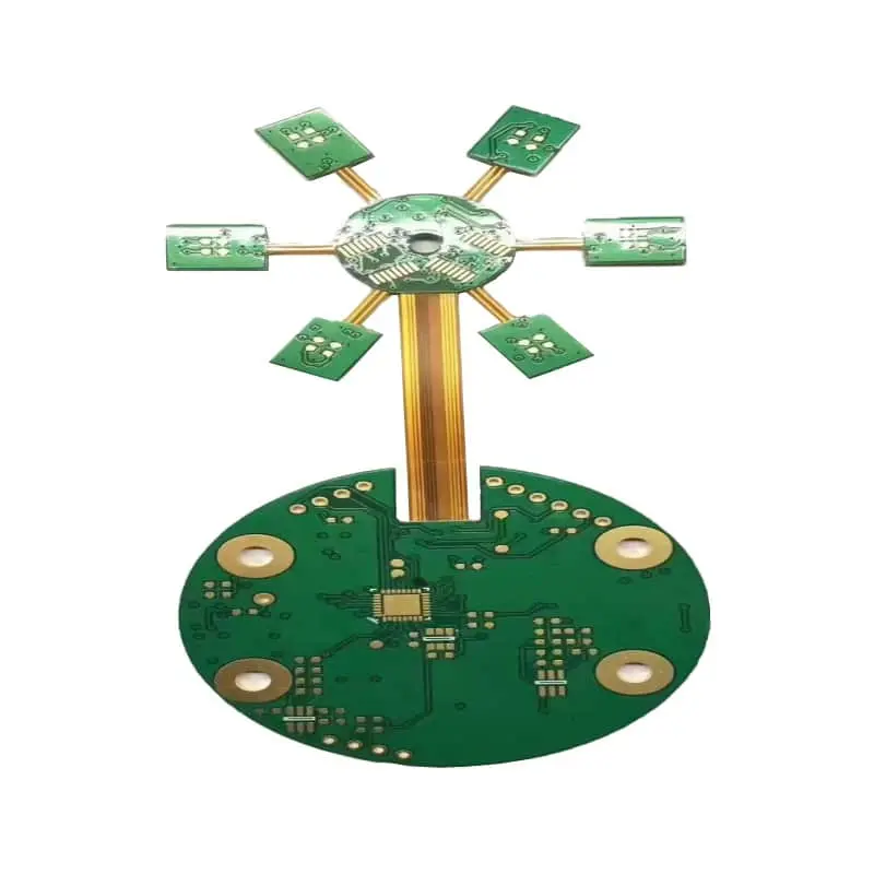
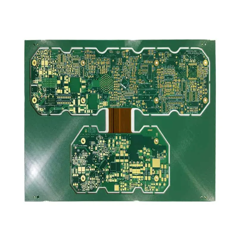
3. Rigid-Flex & Heavy Copper PCB Manufacturing
Demand for rigid-flex PCBs is surging in 2026 for aerospace, automotive, and medical applications, thanks to their shock resistance, flexibility, and compact packaging. Our rigid-flex process improves lamination consistency and alignment accuracy, supporting rigid-flex structures up to 20 layers with reliable bending cycles exceeding 10,000 times.
For high-power uses like EV powertrains and industrial power supplies, we offer 6–10 oz+ heavy copper PCBs with embedded copper blocks and protrusion technologies for better heat dissipation. Through-hole plating achieves an aspect ratio of 20:1, ensuring stable electrical connections in thick, high-power boards.
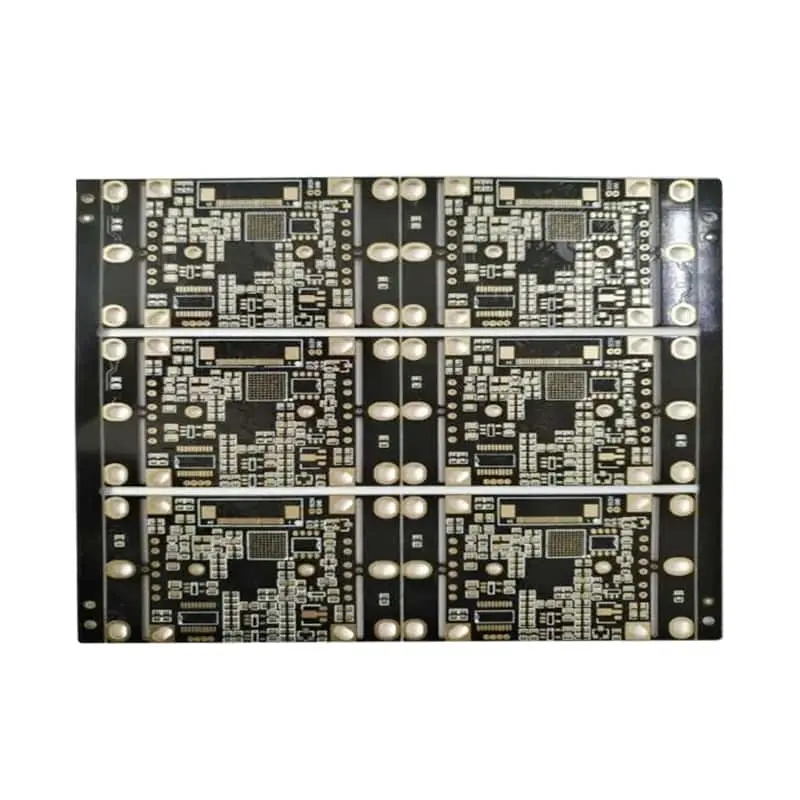
4. AI-Driven Smart Manufacturing & Quality Control
Smart automation and digitalization define PCB production in 2026. HAODA ELECTRONIC CO., LIMITED has integrated AI systems across its entire production line:
- AI process monitoring: Real-time tracking of lamination, etching, and plating parameters to eliminate defects and ensure batch consistency
- Machine vision AOI: 100% inspection of traces, microvias, and solder mask, detecting micro defects ≤ 0.05 mm invisible to the human eye
- Full traceability: Unique ID for every PCB, with real-time tracking of materials, processes, and test results to meet medical (ISO 13485) and automotive (IATF 16949) compliance
This smart manufacturing model cuts production defects by 40% and shortens lead times by 25%, keeping quality consistent for both prototypes and high-volume orders.
5. Sustainable Green Manufacturing
Sustainability is now a must in the electronics industry in 2026. Our custom PCB service uses fully eco-friendly production:
- Lead-free & halogen-free materials: All substrates and solder masks meet RoHS and REACH standards
- Water & energy recycling: 85% process water recovery, 30% energy recovery, and 20% lower carbon emissions
- Scrap recycling: Partnerships with certified recyclers for 100% processing of production waste to minimize environmental impact
Why Choose HAODA ELECTRONIC CO., LIMITED for Your Custom PCB Manufacturing?
As an experienced professional PCB manufacturer, HAODA ELECTRONIC CO., LIMITED combines 2026’s latest technologies with customer-first service to deliver unbeatable value:
- Top-tier technical capabilities: Mastery of M9/M10 high-frequency materials, 7-level HDI, rigid-flex, heavy copper, and more
- Flexible order support: From 1-piece prototypes to 100,000+ pieces mass production; fast turnaround (prototypes in 24 hours, mass production in 3–5 days)
- Strict quality assurance: Compliant with IPC Class 3, ISO 9001, ISO 13485, IATF 16949; 100% electrical testing and AOI inspection
- Trusted worldwide: Serving 500+ customers across 30+ countries in AI, automotive, medical, communications, and other industries
- One-stop service: DFM review, design optimization, manufacturing, assembly, and testing to simplify your supply chain
Closing
In 2026, custom PCB manufacturing is the key to unlocking electronic innovation — and HAODA ELECTRONIC CO., LIMITED is your reliable partner for navigating industry change. We combine ultra-low-loss high-frequency materials, AI-driven smart manufacturing, and other cutting-edge technologies to deliver custom PCBs that meet the highest standards for performance, precision, and reliability.
Whether you’re developing an AI server backplane, 5G RF board, medical wearable, or automotive power PCB, our expert engineering team and advanced production lines can turn your design vision into reality. Contact HAODA ELECTRONIC CO., LIMITED today to discuss your custom PCB needs and start your journey of innovation and success.