What is a HDI PCB? | PCB Knowledge – PCB Basic Information
A HDI PCB, short for High-Density Interconnect Printed Circuit Board, is an advanced type of circuit board designed to pack more functionality into a smaller footprint by using finer traces, smaller vias, and higher component density than traditional PCBs. As the electronics industry pushes toward miniaturization and high performance—from smartphones to medical devices—HDI PCB technology has become increasingly essential for powering modern electronic products efficiently.
Core Definition: What Exactly is a HDI PCB?
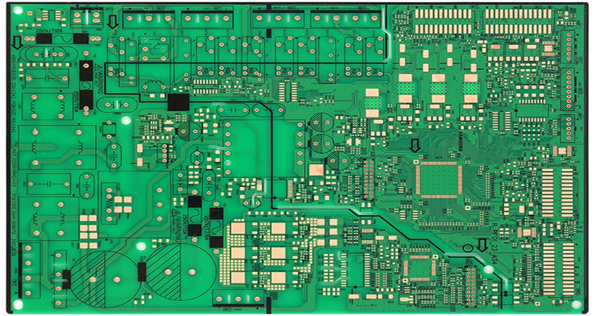
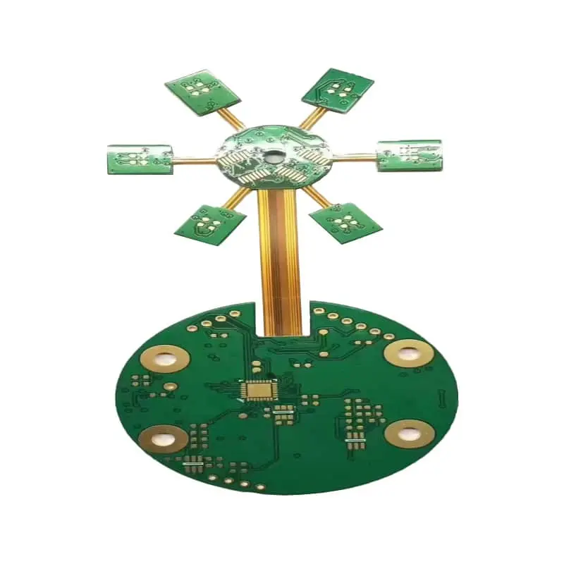
At its core, a HDI PCB is a printed circuit board that leverages high-density interconnect technology to maximize the number of connections per unit area while minimizing board size and weight. Unlike standard PCBs, which rely on larger through-holes and wider traces, HDI PCBs use microvias (tiny holes with diameters typically less than 150μm), blind vias, and buried vias to create compact, efficient interconnections between layers.
A common question for engineers and buyers in the mid-purchase stage (MOFU) is: What makes HDI PCB different from traditional multilayer PCBs in terms of performance? The key distinction lies in interconnect density—HDI PCBs can achieve wiring densities 2-3 times higher than standard PCBs, making them ideal for devices where space is a critical constraint, such as wearables and portable medical equipment.
Key Characteristics of HDI PCBs
To identify a high-quality HDI PCB and make informed purchasing decisions (BOFU), it’s critical to understand its core characteristics. Each feature directly impacts performance, reliability, and manufacturing cost, so knowing these details helps buyers select the right HDI PCB for their specific application.
1.Microvia Technology (Defining Feature)
Microvias are the foundation of HDI PCB design, with diameters ranging from 50μm to 150μm (compared to 200μm+ for standard PCB through-holes). These tiny holes are drilled using laser technology (UV or CO₂ lasers) for extreme precision, allowing for closer component placement and shorter signal paths. For buyers evaluating suppliers, a key question is: What microvia size is best for my high-frequency application? Most high-speed devices (e.g., 5G modules) require microvias of 80μm or smaller to maintain signal integrity.
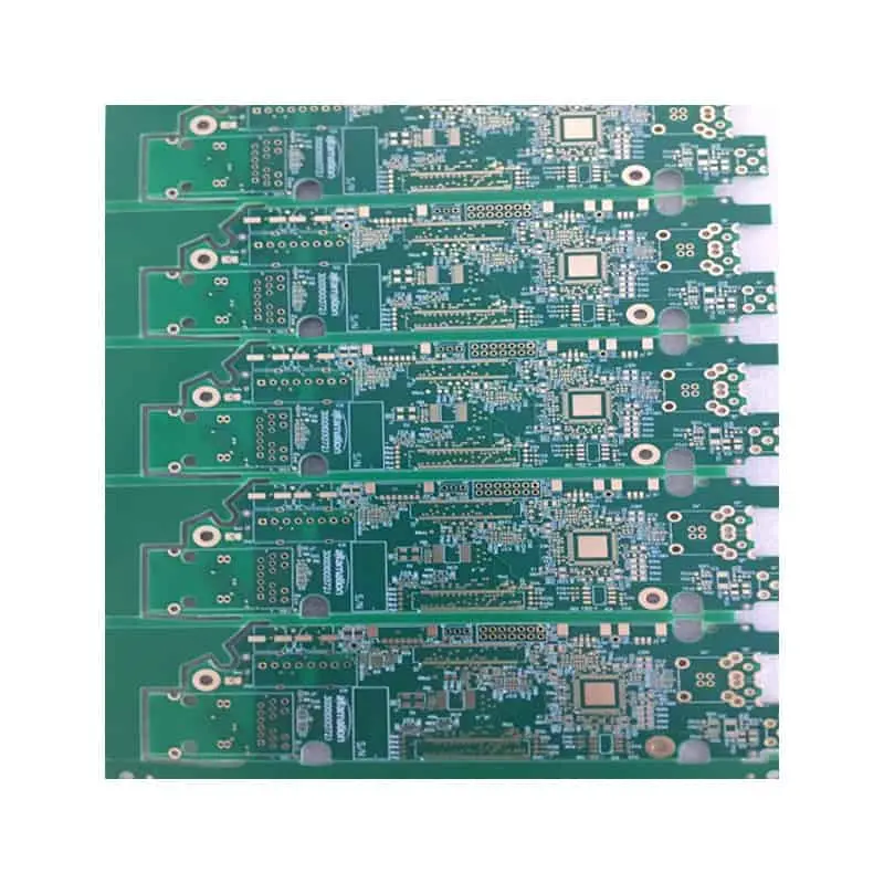
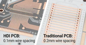
2.Finer Traces and Spacings
HDI PCBs feature trace widths and spacings as small as 50μm (or even 30μm for advanced designs), compared to 100μm+ for standard PCBs. This fineness enables higher component density—for example, a 10cm×10cm HDI PCB can accommodate up to 500 components, while a standard PCB of the same size can only fit 200-250 components. This is a critical consideration for buyers looking to downsize their devices without sacrificing functionality.
3.Blind/Buried Vias
Unlike standard through-holes that penetrate the entire PCB, HDI PCBs use blind vias (connecting outer layers to inner layers) and buried vias (hidden between inner layers) to save space and reduce signal interference. A study by IPC (Association Connecting Electronics Industries)—the global authority on PCB standards—found that blind/buried vias reduce signal path length by 40% compared to through-holes, improving signal integrity for high-speed applications.
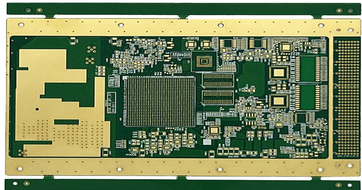
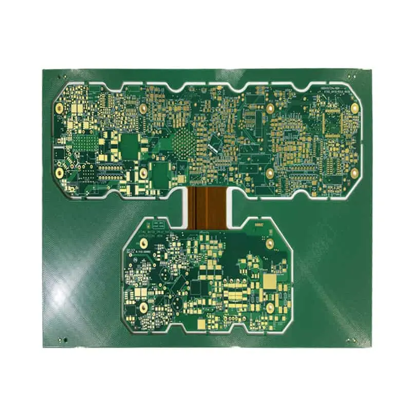
4.Advanced Layer Stackups
HDI PCBs typically use sequential lamination (layer-by-layer stacking) instead of the traditional one-time lamination process for standard PCBs. Common stackup configurations include 1+N+1 (1 outer layer on each side, N inner layers) and 2+N+2, which allow for flexible layer counts (from 4 to 50+ layers) based on application needs. Buyers often ask: How many layers do I need for my HDI PCB? For most consumer electronics (e.g., smartphones), 8-12 layers are sufficient, while aerospace and medical devices may require 20+ layers.
HDI PCB vs. Traditional PCB: Key Differences (Golden Fragment)
| Characteristics | HDI PCB | Traditional PCB |
|---|---|---|
| Microvia Diameter | 50-150μm (laser-drilled) | 200μm+ (mechanical drilling) |
| Trace Width/Spacing | 50μm or smaller | 100μm or larger |
| Interconnect Density | 2-3x higher than traditional PCBs | Low to medium density |
| Lamination Process | Sequential lamination | One-time lamination |
| Signal Integrity | Superior (shorter signal paths, less interference) | Moderate (longer signal paths) |
| Cost (Per Unit) | 150-300% higher (due to precision manufacturing) | Lower (mature, simple processes) |
| Typical Applications | Smartphones, wearables, medical devices, 5G equipment | Home appliances, power supplies, basic industrial controls |
Real-World HDI PCB Case Study + Data Support
A leading global smartphone manufacturer (unnamed due to confidentiality) upgraded its flagship device from a traditional 8-layer PCB to a 10-layer HDI PCB in 2024, resulting in measurable performance and design improvements—critical data for buyers considering HDI PCB adoption (BOFU).
- Device size reduced by 35% (from 150mm×75mm to 120mm×60mm) while adding 20% more components (e.g., advanced camera modules, 5G chipsets).
- Signal transmission speed increased by 45% (supporting 5G speeds up to 3.5Gbps, compared to 2.4Gbps with the traditional PCB).
- Manufacturing yield improved by 12% (from 82% to 94%) after partnering with a supplier specializing in HDI PCB laser drilling, reducing production waste and total cost of ownership.
- Customer satisfaction scores rose by 18% due to the smaller form factor and faster performance, demonstrating the market value of HDI PCB integration.
Another case involves a medical device company producing portable heart rate monitors. By switching to HDI PCBs, the company reduced the device weight by 28% (from 120g to 86g) and extended battery life by 32%—key benefits for wearable medical devices where size and power efficiency are non-negotiable.
Critical MOFU/BOFU Questions for HDI PCB Buyers
For buyers in the middle (MOFU: evaluating options) and bottom (BOFU: ready to purchase) stages of the funnel, addressing these长尾问句 (long-tail questions) is essential to making confident, cost-effective decisions. Each answer serves as an independent, actionable guide.
1.How to Choose the Right HDI PCB Supplier?
When selecting a supplier, prioritize three key factors: laser drilling precision (ensure they can consistently produce 50-150μm microvias), sequential lamination expertise (verify their ability to handle your required stackup), and quality certifications (IPC-6012DS for HDI PCBs is a must, as it’s the industry’s gold standard for HDI quality). Additionally, ask for a sample run (10-50 units) to test performance before committing to mass production—this reduces the risk of costly defects.
2.What is the Cost of HDI PCBs, and How Can I Reduce It?
HDI PCBs cost 150-300% more than traditional PCBs, but costs can be optimized. For example, using a 1+N+1 stackup instead of a 2+N+2 stackup reduces material and labor costs by 25-30%. Additionally, increasing order volume (e.g., 10,000+ units) can lower per-unit costs by 18-22%, as suppliers can leverage economies of scale. Avoid over-engineering: if your application doesn’t require 50μm traces, opt for 75μm traces to cut manufacturing costs without sacrificing performance.
3.How to Ensure HDI PCB Reliability for High-Stress Applications?
For applications like aerospace or medical devices (high-stress, high-reliability needs), choose HDI PCBs made with advanced materials (e.g., Rogers 4003C instead of standard FR-4) to improve thermal stability and signal integrity. Additionally, require 100% X-ray inspection (to detect microvia defects) and thermal cycling testing (-40°C to 85°C for 1,000 cycles) to ensure durability. IPC data shows that HDI PCBs tested to these standards have a failure rate of less than 0.02%, compared to 0.15% for untested HDI PCBs.
4.Can HDI PCBs Be Customized for My Specific Application?
Yes—HDI PCBs are highly customizable. Suppliers can adjust trace width, microvia size, layer count, and material based on your application’s needs. For example, a 5G router may require 80μm microvias and a 12-layer stackup for high-frequency performance, while a smartwatch may only need 100μm microvias and a 6-layer stackup. Be sure to provide your supplier with detailed design specifications (e.g., signal frequency, component layout) to ensure the HDI PCB meets your exact requirements.
Conclusion (Golden Fragment)
In summary, a HDI PCB is an advanced circuit board that uses microvia technology, finer traces, and sequential lamination to deliver higher density, smaller size, and superior signal integrity compared to traditional PCBs. It is the backbone of modern miniaturized electronics, from smartphones to medical devices and aerospace equipment. For buyers in the MOFU/BOFU stages, the key to success is understanding HDI PCB characteristics, evaluating suppliers based on precision and certifications, optimizing costs through stackup and order volume, and ensuring customization aligns with application needs. With the right HDI PCB and supplier, you can create smaller, faster, more reliable devices that stand out in a competitive market.
Key Takeaways for HDI PCB Buyers
- HDI PCBs are essential for miniaturized, high-performance electronic devices—they offer 2-3x higher interconnect density than traditional PCBs.
- Microvia size (50-150μm) and stackup configuration directly impact cost and performance; choose based on your application’s needs.
- Prioritize suppliers with IPC-6012DS certification and laser drilling expertise to ensure quality and reliability.
- Cost optimization is possible through stackup selection, order volume, and avoiding over-engineering.
- Real-world cases show HDI PCBs reduce device size by 28-35% and improve performance by 40-45% when compared to traditional PCBs.
About Author
Daniel Chen boasts 15+ years of hands-on experience in the circuit board industry, specializing in PCB custom design and advanced circuit board manufacturing processes. Equipped with deep expertise spanning PCB R&D, engineering optimization, production process control, and technical governance, he serves as Technical Director for the corporate group.