Table of Contents
- Introduction
- What Is Custom PCB Fabrication Service?
- Core Technical Workflow of Custom PCB Fabrication
3.1 Requirement Analysis & DFM Validation
3.2 Material Selection for Custom PCB Performance
3.3 Precision Fabrication Process
3.4 Surface Finish & Protective Coating
3.5 Rigorous Quality Control & Testing
- Key Custom PCB Fabrication Solutions for Diverse Applications
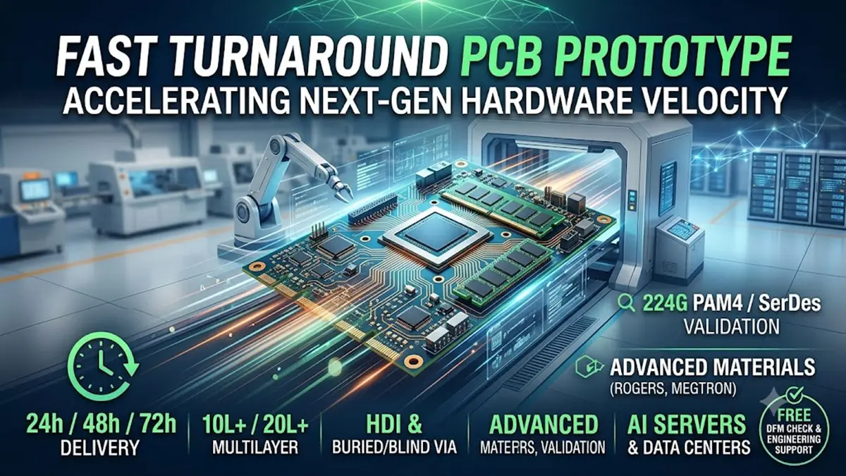
4.1 High-Speed & High-Frequency PCB Solution
4.2 HDI & Miniaturized PCB Solution
4.3 High-Power & Thermal Management PCB Solution
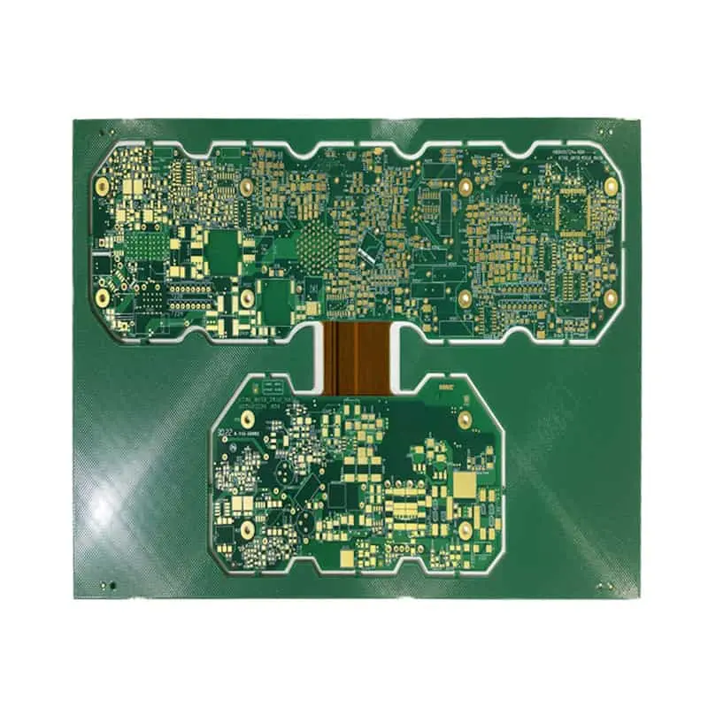
4.4 Rigid-Flex PCB Solution for Wearables
- Why Choose Professional Custom PCB Fabrication Service?
- Conclusion
- FAQ
1. Introduction
In today’s fast-evolving electronics industry, custom PCB fabrication service stands as the cornerstone of product innovation, enabling engineers to translate unique design concepts into high-performance printed circuit boards. Unlike standard off-the-shelf PCBs, custom PCB fabrication delivers tailored solutions that match precise requirements for signal integrity, form factor, thermal resistance, and industry compliance. Whether for prototype validation, small-batch production, or mass manufacturing, a reliable custom PCB fabrication service ensures consistency, quality, and cost-efficiency across all project stages.
The demand for custom PCB solutions continues to surge across sectors like industrial automation, medical devices, 5G communication, and consumer electronics. Each application imposes distinct technical challenges—from high-frequency signal stability in RF devices to miniaturization in wearables—and only a specialized custom PCB fabrication service can address these with optimized materials, precision processes, and expert engineering support. This article explores the technical framework, core processes, and application-specific solutions of professional custom PCB fabrication, adhering to strict quality standards and design best practices.
2. What Is Custom PCB Fabrication Service?
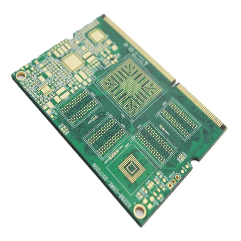
Custom PCB fabrication service refers to a comprehensive manufacturing solution that designs, engineers, and produces printed circuit boards customized to a client’s exact technical specifications. This service covers the entire lifecycle from design file review, material selection, and precision fabrication to quality testing and delivery, ensuring every custom PCB meets performance, reliability, and regulatory requirements.
At its core, custom PCB fabrication differs from generic PCB production in three key aspects:
- Tailored Design: Every custom PCB is optimized for specific electrical, mechanical, and environmental needs—including layer count, trace width, impedance control, and board shape—rather than adhering to standard dimensions.
- Material Flexibility: Custom PCB fabrication service offers a wide range of substrates (FR-4, high-Tg FR-4, Rogers, polyimide, aluminum) and copper thicknesses (0.5oz–4oz) to match application demands.
- Process Customization: Advanced processes like HDI, blind/buried vias, controlled impedance, and selective plating are integrated into custom PCB fabrication to solve complex design challenges.
A professional custom PCB fabrication service also provides value-added support, including DFM (Design for Manufacturability) analysis, design optimization, and technical consultation, ensuring seamless transition from design to production and minimizing costly rework.
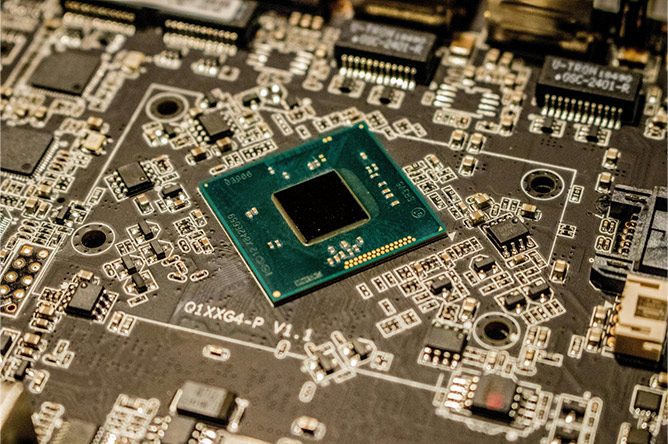
3. Core Technical Workflow of Custom PCB Fabrication
The success of custom PCB fabrication relies on a streamlined, precision-driven workflow that combines engineering expertise, advanced equipment, and strict quality control. Below is the step-by-step technical process that defines reliable custom PCB fabrication service.
3.1 Requirement Analysis & DFM Validation
The first critical stage of custom PCB fabrication service is thorough requirement analysis and DFM validation, which bridges design intent and manufacturing capability. The engineering team collaborates closely with clients to define all technical parameters:
- Electrical requirements: Signal speed, voltage/current load, impedance tolerance (e.g., 50Ω for RF, 90Ω for USB differential lines).
- Mechanical specifications: Board dimensions, thickness (0.4–3.2mm), layer count (1–32 layers), and shape (standard or irregular).
- Environmental conditions: Operating temperature range (-40°C to 125°C), humidity, vibration, and exposure to chemicals.
- Regulatory standards: IPC Class 2/3, UL, ISO 13485 (medical), or IATF 16949 (automotive).
After requirement collection, DFM validation is performed to identify potential manufacturing issues early. This includes checking design rule compliance (minimum line width/spacing: 3/3mil, minimum hole size), verifying Gerber/Excellon file integrity, and optimizing layouts for yield improvement. DFM analysis in custom PCB fabrication service reduces production risks, shortens lead times, and ensures the final custom PCB meets all performance goals.
3.2 Material Selection for Custom PCB Performance
Material selection is a foundational step in custom PCB fabrication, directly impacting the electrical performance, thermal resistance, and durability of the final board. A professional custom PCB fabrication service offers a curated range of materials tailored to application needs:
- Substrates:
- FR-4: Standard glass-reinforced epoxy laminate for general consumer electronics (cost-effective, good insulation).
- High-Tg FR-4: For high-temperature environments (Tg > 170°C), ideal for industrial and automotive custom PCBs.
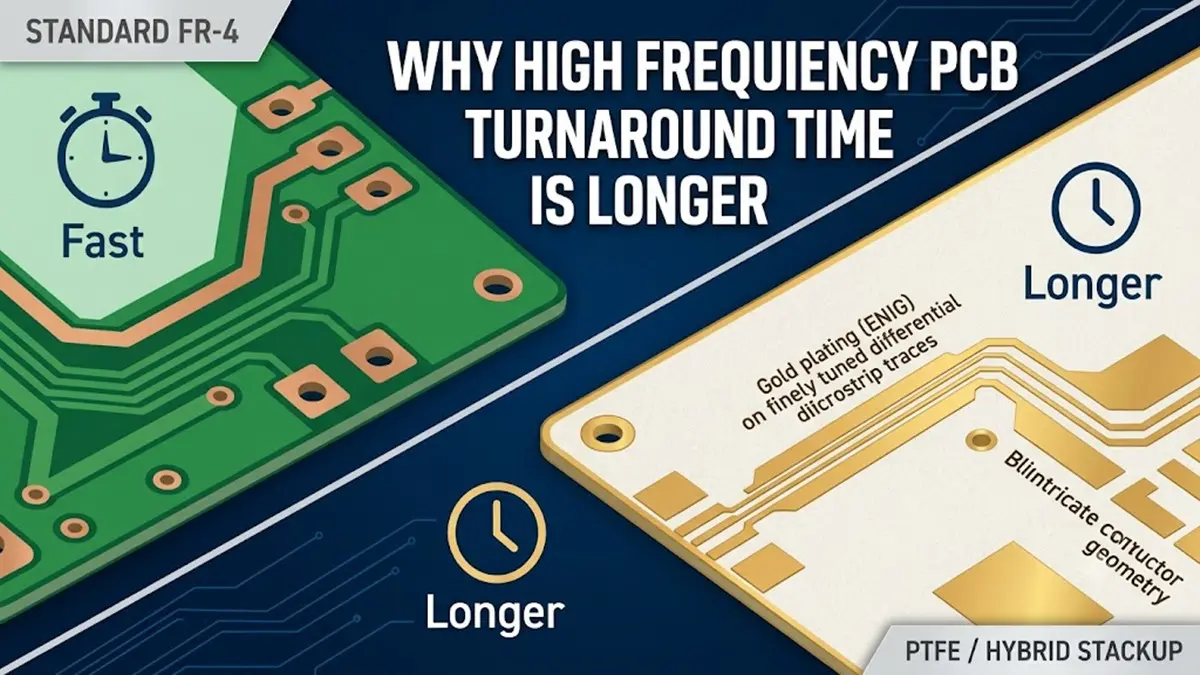
- Rogers/PTFE: High-frequency laminates with low dielectric constant, perfect for 5G, RF, and microwave custom PCB fabrication.
- Aluminum/Copper Core: Metal-core substrates for high-power devices, providing excellent heat dissipation.
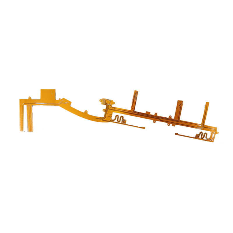
- Polyimide: Flexible substrate for rigid-flex and wearable custom PCBs.
- Copper Foil: Thickness options from 0.5oz (fine traces) to 4oz (high current) to balance conductivity and miniaturization.
- Prepreg: Bonding material for multilayer custom PCBs, ensuring layer adhesion and insulation.
The material selection process in custom PCB fabrication service is data-driven: engineers analyze electrical simulation results, thermal modeling data, and cost constraints to recommend the optimal material combination for each custom PCB project.
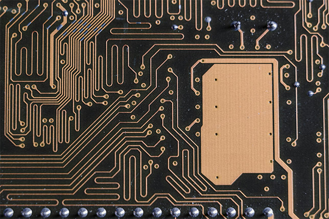
3.3 Precision Fabrication Process
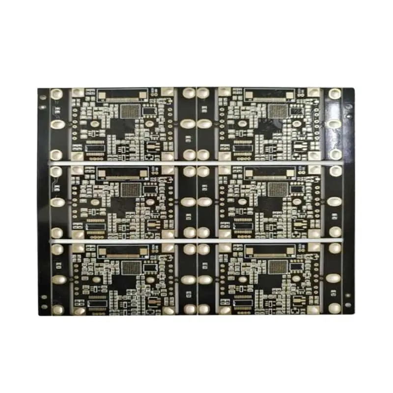
The fabrication stage is where custom PCB fabrication service transforms design files into physical boards, utilizing advanced equipment and precision processes to ensure accuracy. Key steps include:
- Inner Layer Imaging & Etching: For multilayer custom PCBs, inner layer circuits are transferred to copper-clad laminates via photolithography or LDI (Laser Direct Imaging), then etched to remove excess copper.
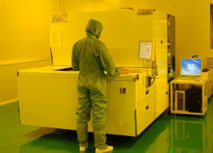
Screen Ledia Ldi Exposure Machine - Layer Lamination: Inner layers, prepreg, and outer copper foils are stacked and bonded under high temperature and pressure to form a multilayer panel.
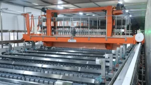
Hx Automation Pcb Plating Line - Drilling & Plating: Holes for vias and through-holes are drilled (laser drilling for micro-vias in HDI custom PCBs), then plated with copper to create conductive pathways between layers.
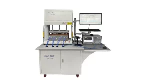
Hisun Test Sif 2001 Automatic Impedance Test System (equipped With Keysight Vna) - Outer Layer Processing: Outer layer circuits are imaged, etched, and inspected via AOI (Automated Optical Inspection) to catch defects like open circuits or short circuits.
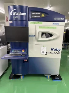
Nordson Dage Xd7600nt X Ray Tester Every step in custom PCB fabrication is monitored with strict process controls: laser alignment ensures layer registration accuracy (±0.01mm), and automated equipment minimizes human error. This precision is critical for high-density custom PCBs, where even minor deviations can cause signal failure.
3.4 Surface Finish & Protective Coating
Surface finish is a critical final step in custom PCB fabrication service, protecting copper traces from oxidation, ensuring solderability, and meeting application-specific requirements. Common surface finishes for custom PCBs include:
- ENIG (Electroless Nickel Immersion Gold): Nickel-gold coating with excellent solderability and corrosion resistance, ideal for high-reliability custom PCBs (medical, aerospace).
- HASL (Hot Air Solder Leveling): Cost-effective leaded/lead-free solder coating for general consumer electronics.
- OSP (Organic Solderability Preservative): Environmentally friendly organic coating for fine-pitch components, suitable for high-volume custom PCB fabrication.
- Immersion Tin/Silver: Thin metal coatings for high-frequency custom PCBs, minimizing signal loss.
In addition to surface finish, protective coatings like solder mask (green, blue, black, or white) are applied to insulate copper traces, prevent solder bridging, and enhance durability. For harsh environments, conformal coating (Parylene, acrylic) is added to resist moisture, dust, and chemicals—an essential feature for industrial and automotive custom PCBs.
3.5 Rigorous Quality Control & Testing
Quality control is non-negotiable in professional custom PCB fabrication service, with multi-stage testing ensuring every custom PCB meets IPC and client specifications. Key quality checks include:
- AOI Inspection: Automated optical scanning to detect defects like missing pads, trace shorts, or solder mask errors.
- Electrical Testing: Flying probe or fixture-based testing for continuity, isolation, and impedance accuracy (critical for high-speed custom PCBs).
- X-Ray Inspection: For multilayer and HDI custom PCBs, X-rays verify internal layer alignment and via plating integrity.
- Thermal Testing: Thermal resistance and temperature cycling tests for high-power custom PCBs.
- Dimensional Verification: Precision measurement of board dimensions, hole sizes, and layer thicknesses.
A reliable custom PCB fabrication service maintains complete traceability for every board, with batch records and test reports available for client review. This commitment to quality ensures that custom PCBs perform reliably in even the most demanding applications.
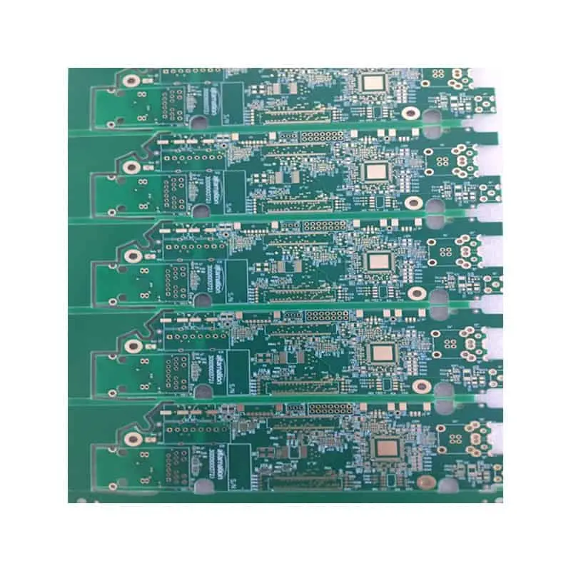
4. Key Custom PCB Fabrication Solutions for Diverse Applications
Custom PCB fabrication service delivers application-specific solutions to address unique technical challenges across industries. Below are the most in-demand custom PCB fabrication solutions, optimized for performance and reliability.
4.1 High-Speed & High-Frequency PCB Solution
High-speed and high-frequency circuits (5G, RF, data centers) require custom PCBs with strict impedance control, low signal loss, and minimal EMI. The custom PCB fabrication solution for these applications includes:
- High-frequency substrates (Rogers, PTFE) with low dielectric constant (Dk < 3.5).
- Controlled impedance routing (±5% tolerance) for differential signals (USB4, PCIe).
- Thin copper foil (0.5oz) and smooth trace edges to reduce skin effect loss.
- Ground plane optimization and shielded traces to minimize crosstalk.
This custom PCB fabrication solution ensures signal integrity at frequencies up to 100GHz, making it ideal for 5G base stations, RF transceivers, and high-speed communication devices.
4.2 HDI & Miniaturized PCB Solution
As devices shrink (wearables, smartphones, medical implants), HDI (High-Density Interconnect) custom PCBs become essential for packing more components into smaller spaces. The HDI custom PCB fabrication solution features:
- Micro-vias (0.1–0.2mm diameter) and blind/buried vias for interlayer connections.
- Fine line width/spacing (2/2mil) and small pad sizes (0.3mm).
- Multilayer stackups (4–16 layers) with high layer registration accuracy.
- Laser drilling and LDI imaging for precision patterning.
HDI custom PCB fabrication enables 30–50% space savings compared to standard multilayer PCBs, making it the top choice for compact, high-performance electronics.
4.3 High-Power & Thermal Management PCB Solution
Industrial power supplies, automotive electronics, and LED lighting require custom PCBs that handle high current and dissipate heat efficiently. The high-power custom PCB fabrication solution includes:
- Thick copper foil (2–4oz) for high current carrying capacity (up to 50A).
- Metal-core substrates (aluminum/copper) or high-Tg FR-4 for thermal resistance.
- Thermal vias and heat sinks integrated into the design to reduce junction temperature.
- Conformal coating for protection in high-temperature industrial environments.
This custom PCB fabrication solution prevents overheating and ensures stable performance under heavy loads, critical for industrial automation and automotive applications.
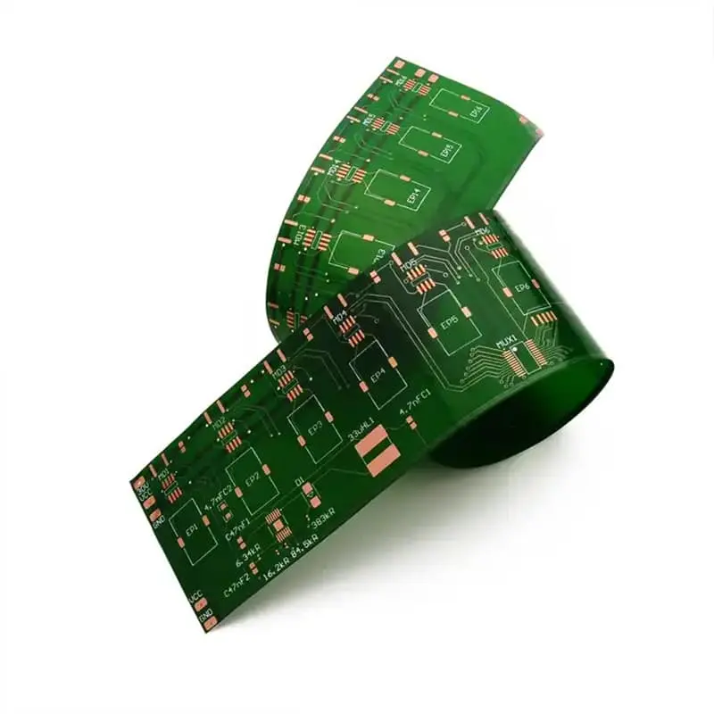
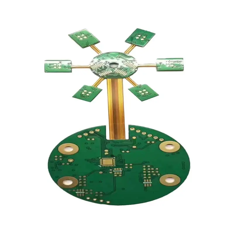
4.4 Rigid-Flex PCB Solution for Wearables
Wearable devices (smartwatches, fitness trackers, medical wearables) demand flexible, lightweight custom PCBs that fit curved surfaces. The rigid-flex custom PCB fabrication solution combines rigid and flexible layers:
- Rigid FR-4 sections for component mounting and flexible polyimide sections for bending (up to 180°).
- Reinforced vias at rigid-flex junctions to prevent cracking during bending.
- Thin profile (0.2–0.5mm) and lightweight construction.
- Biocompatible coatings for medical wearable custom PCBs.
Rigid-flex custom PCB fabrication eliminates bulky connectors and enables seamless integration into wearable designs, driving innovation in consumer and medical electronics.
5. Why Choose Professional Custom PCB Fabrication Service?
Partnering with a professional custom PCB fabrication service provider offers significant advantages over in-house production or generic manufacturers:
- Expert Engineering Support: Experienced engineers provide DFM analysis, design optimization, and technical consultation, solving complex challenges and ensuring design feasibility.
- Advanced Manufacturing Capabilities: Access to state-of-the-art equipment (LDI, laser drilling, AOI) and specialized processes (HDI, rigid-flex, controlled impedance) that in-house facilities often lack.
- Strict Quality Assurance: Comprehensive testing and IPC compliance guarantee reliable, defect-free custom PCBs, reducing the risk of product failure.
- Flexible Production Scales: Support for prototype (1–10 units), small-batch (100–5,000 units), and mass production (10,000+ units) with consistent quality.
- Cost & Time Efficiency: Optimized material usage, streamlined workflows, and reduced rework lower overall costs; reliable lead times (24-hour prototypes, 5–7 days for batches) accelerate time-to-market.
- Industry Compliance: Adherence to global standards (UL, ISO, IPC) ensures custom PCBs meet regulatory requirements for medical, automotive, and aerospace applications.
A trusted custom PCB fabrication service provider acts as a long-term technical partner, supporting product development from concept to mass production and enabling businesses to stay competitive in a rapidly evolving industry.
6. Conclusion
Custom PCB fabrication service is more than just a manufacturing solution—it is a catalyst for electronic innovation, delivering tailored printed circuit boards that meet the most demanding performance, reliability, and miniaturization requirements. From initial requirement analysis and DFM validation to precision fabrication, surface finishing, and rigorous quality control, every stage of the custom PCB fabrication workflow is optimized for accuracy, consistency, and efficiency.
With application-specific solutions for high-speed, HDI, high-power, and rigid-flex designs, professional custom PCB fabrication service empowers engineers to push the boundaries of electronic design across industries. By partnering with an experienced provider, businesses gain access to expert engineering, advanced technology, and strict quality assurance—all while reducing costs and accelerating time-to-market.
As electronics continue to evolve toward higher speeds, smaller sizes, and greater reliability, custom PCB fabrication service will remain an indispensable foundation for innovation, enabling the next generation of smart, connected devices.
7. FAQ
Q1: What file formats are required for custom PCB fabrication?
A: Standard files include Gerber (RS-274X), Excellon drill files, IPC netlist, and board outline files. Some providers also accept ODB++ or IPC-2581 formats.
Q2: What is the typical lead time for custom PCB fabrication?
A: Prototypes (1–10 units) take 24–72 hours; small batches (100–5,000 units) take 5–7 days; mass production takes 7–14 days. Expedited services are available for urgent projects.
Q3: What is the minimum line width/spacing for custom PCBs?
A: Standard capabilities are 3/3mil; advanced HDI custom PCB fabrication supports 2/2mil or finer for high-density designs.
Q4: Can custom PCB fabrication service support special shapes or sizes?
A: Yes. Professional providers can fabricate custom PCBs with irregular shapes, cutouts, and sizes up to 1800×800mm for single-sided boards.
Q5: What certifications should a reliable custom PCB fabrication provider have?
A: Look for ISO 9001 (quality management), UL (safety), IPC Class 2/3 (performance), and industry-specific certifications like IATF 16949 (automotive) or ISO 13485 (medical)。
About Author
David Chen https://www.linkedin.com/in/pcbcoming/
David Chen boasts an extensive professional background in PCBA manufacturing, PCBA testing, and PCBA optimization, with specialized expertise in high-precision PCBA fault analysis and rigorous PCBA reliability testing. Skilled in complex circuit design and cutting-edge advanced PCB manufacturing processes, he delivers solutions that elevate product durability and performance across industrial applications. His technical articles focusing on PCBA manufacturing workflows and testing methodologies are widely cited by industry peers, research institutions, and technical platforms, solidifying his reputation as a recognized technical authority in the global circuit board manufacturing sector.