Fast Turnaround PCB Prototype: Accelerating Next-Gen Hardware Velocity
What Is a Fast Turnaround PCB Prototype and How Does It Compare to Standard Production?
| PCB Parameter | Fast Turnaround Protocol | Standard Production Run |
|---|---|---|
| Lead Time (2-4 Layers) | 24 Hours | 5 – 7 Business Days |
| Lead Time (6-12 Layers) | 48 Hours | 7 – 10 Business Days |
| Lead Time (14-24+ Layers) | 72 Hours | 10 – 15 Business Days |
| CAM Verification Window | Immediate (<2 Hours) | 12 – 24 Hours |
| Material Availability | In-Stock Advanced Stack | Just-In-Time Ordering |
Why Is Quick-Turn Prototyping Critical for High-Speed Systems and AI Servers?
Scenario-Driven Analysis & Manufacturing Pain Points
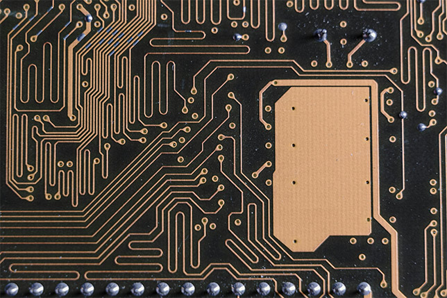
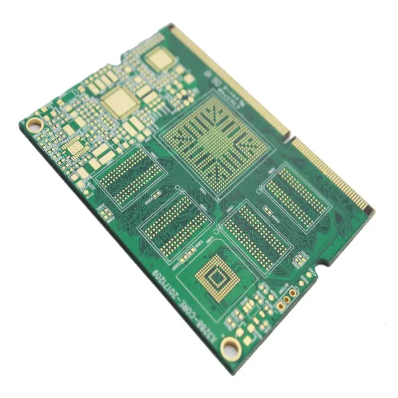
In the hyper-competitive AI infrastructure sector, missing a product launch window by a single month can erode market share and millions in potential revenue . Designers engineering an AI server accelerator board face massive layout complexities . They must route thousands of differential pairs coming off high-pin-count BGA chips while dealing with dense power rails.
The Crucial Manufacturing Pain Point: When working with layer counts exceeding 16 layers at tight pitches, standard prototype shops often struggle with layer-to-layer registration accuracy . During the rapid lamination cycle required for fast turnaround, material shift can cause internal misregistration This misalignment can induce devastating impedance discontinuities or blind/buried via fracturing along the Z-axis, completely ruining the prototype.
What Advanced Technical Capabilities Facilitate Rapid PCB Prototyping Without Sacrificing Quality?
Expert Engineering Experience & Parameters
To flawlessly execute a 48-hour turn on a complex 12-layer board, a fabricator must skip traditional film photolithography entirely. Using Laser Direct Imaging (LDI) lets us hit a strict line/space tolerance of ±{10}% on a 3 mil / 3 mil specification.
For high-speed links utilizing 224G PAM4 signaling protocols, skin effect losses and copper surface roughness become major issues. Our engineering standard relies on using ultra-low-loss laminates like Panasonic Megtron 6/7 or Rogers RO4000 series, combined with VLP2 (Very Low Profile, Rz ≤ 1.5 µm) or HVLP copper foils.
| Technical Parameter | Capability Rating |
|---|---|
| Max Layer Count (Quick-Turn) | Up to 32 Layers |
| Minimum Line Width / Space | 2.0 mil / 2.0 mil (50 µm / 50 µm) |
| Registration Accuracy | ±{1} mil (±{25} µm) across the entire panel |
| Impedance Control Tolerance | ±{5}% (Tight) or ±{10}% (Standard) |
| Laser Drill Microvia Aspect Ratio | 1:1 aspect ratio max for reliable plating Furthermore, managing signal integrity on 224G PAM4 architectures requires precise control over via stubs . Our automated backdrilling capability safely removes unused via stubs within a targeted depth tolerance of ±{2} mils, eliminating destructive signal reflections at high frequencies. |
In Which Real-World Applications Is Fast Turnaround PCB Prototyping Indispensable?
Application Environments
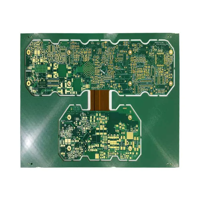
- AI Server Mainboards & Backplanes: These large-form-factor boards exhibit high layer counts (20L to 32L) and heavy copper requirements for power stages . Prototyping validates thermal dissipation under maximum TDP loads.
- Next-Gen Data Center Switches: High-performance routing engines carrying SerDes channels require verification of insertion loss and return loss budgets.
- ADAS Compute Modules: Combining high-speed processing with dense sensor-fusion inputs, these automotive boards demand IPC Class 3 structural integrity combined with ultra-compact HDI microvia processing.
How Can Designers Optimize Design for Manufacturing (DFM) to Prevent Prototyping Delays?
Hardened Engineering Optimization Rules
What Specific Factors Impact the Lead Time of a Fast Turnaround PCB?
| Process Attribute | Standard Impact Time | High-Velocity Alternative |
|---|---|---|
| Stacked HDI (2+N+2) | Adds 24 – 48 Hours | Staggered Microvias |
| Electroless Nickel OSP | Standard Process Time | HASL or ENIG (Streamlined) |
| Controlled Backdrilling | Adds 4 – 6 Hours | Optimized Via Stack Design |
How Do You Select a Reliable Quick-Turn PCB Prototyping Partner?
Evaluation Criteria
Look for a partner that displays an open, transparent supply chain and live manufacturing metrics . A true fast-turnaround facility will have dedicated quick-turn fabrication cells completely isolated from high-volume production lines . This prevents your prototype order from getting bottlenecked behind large, multi-week production runs.
How Can Engineering Teams Successfully Balance Velocity with Prototyping Budgets?
Cost Analysis Focus
Expediting a complex layout to a 24-hour delivery window carries a premium cost due to dedicated line scheduling and manual logistics handling. If your team does not have assembly components ready on the bench the following morning, choosing a 48-hour window provides a better balance of cost and speed . Additionally, running a comprehensive DFM check reduces the risk of needing a second prototype batch, cutting overall project development expenses.
Case Study: Validating a 12-Layer AI Server Component Within 48 Hours
Engineering Project Breakdown
An engineering team was experiencing severe signal attenuation on their 112G SerDes communication lanes . They needed to test an alternative routing layout and material stackup immediately.
- The Blueprint: A 12-layer board layout using Panasonic Megtron 6 laminate, specifying a 4.5 mil target single-ended impedance profile and a 90 Ω differential pair configuration.
- The Execution: The data package arrived via ODB++ format at 08:00 AM on Day 1 . Automated CAM software validated the trace geometries within 45 minutes . LDI systems exposed the inner layer patterns, and a controlled vacuum lamination cycle completed by 06:00 PM . On Day 2, the panels went through automated mechanical drilling, high-precision backdrilling for stub elimination, and vertical continuous plating.
- The Result: Following automated optical inspection (AOI) and flying-probe electrical verification, the finished prototype boards were packaged and shipped by 08:00 AM on Day 3, achieving a true 48-hour turnaround with an exact ±{7}% impedance variance across all measured channels.
Accelerate Your Hardware Innovation Cycle Today
Partnering with an expert manufacturer gives you access to precision engineering capabilities, instant DFM reviews, and dependable delivery timelines. Ready to accelerate your next hardware iteration?
Upload your design files now to receive an accurate, comprehensive technical quote and DFM evaluation.
Frequently Asked Questions (FAQ)
1. What is the difference between choosing ENIG vs. HASL surface finish for a fast-turn prototype?
Electroless Nickel Immersion Gold (ENIG) offers a flat surface finish (Rz < 0.5 µm), making it ideal for high-density, fine-pitch BGA components . Lead-Free Hot Air Solder Leveling (HASL) can result in an uneven surface finish that may complicate precise component placement during assembly . For high-speed or fine-pitch applications, ENIG is generally preferred despite its slightly higher cost
2. Can a 24-hour fast turnaround accommodate blind and buried via structures?
A 24-hour delivery is usually limited to through-hole designs or simple multi-layer structures . Blind and buried via designs require multiple sequential lamination and drilling stages . These extra steps typically require a minimum of 48 to 72 hours to ensure correct alignment and reliable copper plating
3. How does utilizing ODB++ data format improve turnaround times compared to Gerber RS-274X?
Gerber RS-274X files only contain pure vector graphic data, requiring the CAM engineer to manually define layer orders, drill associations, and netlist attributes . ODB++ inherently structures this technical data into a single package . This allows automated CAM tools to process your design data much faster and eliminates manual data entry steps
4. What tolerance variations should I expect on controlled impedance traces during a quick-turn run?
Our standard processing window delivers an industry-standard ±{10}% impedance tolerance . For challenging designs, such as high-frequency AI hardware pipelines, we can narrow this variance down to ±{5}% . Achieving this requires tightening our etching controls and using specialized, high-grade base laminates
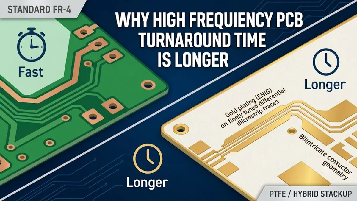
5. Why do high-frequency materials like Rogers RO4003C impact the prototype delivery timeline?
Standard FR4 laminates are stocked in volume and process easily on automated lines[. Specialized materials like Rogers RO4003C or PTFE-based blends require different drill bit feed speeds, specialized plasma de-smear cycles, and unique lamination temperatures . Keeping these premium materials directly in stock allows us to run these advanced boards without extending the quick-turn schedule。
About Author
David Chen https://www.linkedin.com/in/pcbcoming
David Chen boasts an extensive professional background in PCBA manufacturing, PCBA testing, and PCBA optimization, with specialized expertise in high-precision PCBA fault analysis and rigorous PCBA reliability testing. The author has worked with high-layer-count server PCB fabrication, ultra-low-loss backplane stackups, and thermo-mechanical reliability optimization for AI infrastructure projects involving 112G and 224G PAM4 architectures. Skilled in complex circuit design and cutting-edge advanced PCB manufacturing processes, he delivers solutions that elevate product durability and performance across industrial applications. His technical articles focusing on PCBA manufacturing workflows and testing methodologies are widely cited by industry peers, research institutions, and technical platforms, solidifying his reputation as a recognized technical authority in the global circuit board manufacturing sector.