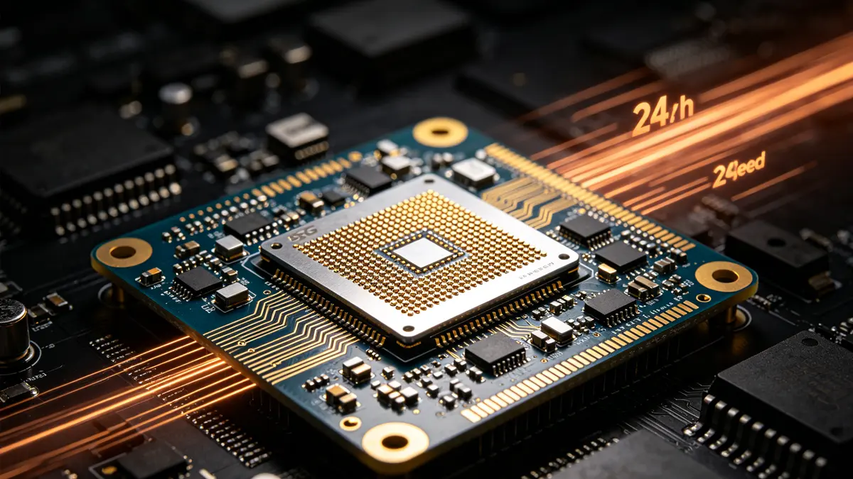
High-frequency PCBs require 30% to 50% longer turnaround times than standard FR-4 boards because their specialized PTFE or thermoset materials demand ultra-precise CNC drilling controls, slower chemical processing cycles, and mandatory plasma desmear steps to prevent delamination and maintain strict signal integrity.
Why Do PTFE and Ceramic-Filled Substrates Extend Lead Times?
The Direct Answer
Specialized high-frequency laminates (such as Rogers, Taconic, or Megtron) have vastly different mechanical and thermal properties than standard FR-4, forcing fabrication plants to abandon high-speed automated processing in favor of highly customized, slower, and strictly monitored manufacturing parameters.
Detailed Manufacturing Pain Points & Material Dynamics
Standard FR-4 relies on a robust, predictable fiberglass matrix bound by epoxy resin. High-frequency boards utilize Teflon (PTFE) or hydrocarbon ceramic-filled chemistries to achieve a low Dissipation Factor ($D_f \le 0.002$) and a stable Dielectric Constant ($D_k$).
However, PTFE is notorious for its “cold flow” characteristic—it is soft, easily deformed under mechanical pressure, and possesses a high Coefficient of Thermal Expansion ($CTE$ in the Z-axis can exceed $200 \text{ ppm/}^\circ\text{C}$ before glass transition).
Dimensional Instability: When baking or pressing a pure PTFE core, the material shifts. Fabricators must introduce a non-standard “pre-scaling” factor in CAM layout. If a standard FR-4 board scales at 100%, a PTFE board might require a shifting matrix of up to 0.05% to 0.08% dynamically across the X/Y axes to ensure pads align after lamination. This trial-and-error scaling calculation adds 4 to 8 hours of engineering verification upfront.
The Lamination Dilemma: Standard FR-4 cures beautifully at $180^\circ\text{C}$ under $300 \text{ psi}$ for a 60-minute press cycle. High-frequency thermoset or thermoplastic materials require lamination temperatures reaching up to $350^\circ\text{C}$ to $370^\circ\text{C}$ and pressures up to $500 \text{ psi}$. A standard multi-layer press cannot reach these profiles. Fabricators must schedule specific high-temperature vacuum presses, and the cooling cycle alone must be painstakingly throttled at less than $1.5^\circ\text{C}$ per minute to prevent internal stress fractures. This expands a standard 2-hour lamination cycle into a 5-to-7-hour bottleneck.
How Does Advanced Drilling and Via Preparation Delay the Line?
The Direct Answer
Mechanical drilling of high-frequency materials requires a radical reduction in feed rates, frequent tool replacements, and a mandatory, specialized plasma etching process to clean the hole walls before copper plating can even begin.
Original Engineering Experience & Parameters
In standard FR-4 production, a single carbide drill bit can rapidly punch through 2,000 to 3,000 holes at a chip load of $3.0 \text{ mils/rev}$ before dulling. If you apply those same parameters to a ceramic-filled high-frequency laminate, the drill bit will snap or melt the material within 100 hits.
Expert Engineering Insight: “When transitioning a high-layer count RF backplane to the drilling floor, we treat the substrate like glass, not plastic. Ceramic fillers are intensely abrasive. We must drop our drill bit hit-count limit down to a maximum of 300 hits per tool, and reduce our feed rates by up to 40% (down to roughly $1.2 \text{ to } 1.5 \text{ mils/rev}$). Furthermore, the ‘smearing’ of soft PTFE resin along the inner copper connections cannot be removed by standard chemical permanganate desmear lines used for FR-4. It requires a dedicated CF4/O2 plasma desmear cycle.”
Drilling Parameter Comparison:
Standard FR-4:   [=========== 100% Speed ===========] -> 3,000 Hits/Bit -> Chemical Desmear
High-Freq PTFE:  [==== 40% Speed ====] -> 300 Hits/Bit -> Plasma Desmear (Adds 4 Hours)
The plasma desmear process is a major turnaround killer. It is a batch process conducted under vacuum conditions inside a specialized RF plasma chamber. The cycle lasts anywhere from 90 to 180 minutes. Because the throughput of a plasma chamber is limited to just a few panels per batch, a high-volume multi-layer RF run creates an immediate operational logjam that adds at least 24 to 48 hours to the total production time.
Why Does Hybrid Stacking and Multi-Step Lamination Create a Bottleneck?
The Direct Answer
Modern high-frequency designs frequently employ hybrid stacking—combining FR-4 and RF substrates in a single board—which forces the factory to execute multiple, sequential lamination cycles instead of a single press run.
Detailed Scenario-Based Analysis
Consider an AI server backplane handling both high-speed 112G/224G PAM4 signaling paths and low-speed digital control lines. To control costs, engineers design a 24-layer hybrid stackup: Layers 1 to 4 and 21 to 24 use an ultra-low-loss material (e.g., Megtron 6 or Rogers RO4003C), while the internal core layers (Layers 5 to 20) utilize standard high-Tg FR-4.
The Scenario: The manufacturing floor cannot press all 24 layers simultaneously. Because the FR-4 prepreg and the Rogers core require completely different curing temperatures and pressures, a sequential lamination process must be utilized.
The Workflow Penalty: 1. The inner FR-4 core (Layers 5-20) is pressed, cured, drilled, and plated first. (Time: 24 hours)
2. The outer high-frequency layers are aligned, prepped with a specialized bonding film (like Rogers Speedboard or 4450F), and sent back to the lamination press for a second cycle. (Time: An additional 18 hours)
3. The final composite board is then drilled again for blind/buried vias and through-holes. (Time: 12 hours)
Every extra lamination cycle multiplies the risk of inner-layer misregistration. A 0.1mm misregistration on a high-frequency line can completely destroy the impedance target ($50\Omega \pm 5\%$). To mitigate this, engineers must pause production to run automated optical inspections (AOI) and X-ray coordinate verifications between every single press step.
Why Do Tight Impedance and Surface Finish Requirements Slow Down Final QC?
The Direct Answer
High-frequency boards mandate ultra-tight impedance tolerances ($\pm5\% \text{ or } \pm 7\%$) and skin-effect-optimized surface finishes like ENIG or ENEPIG, requiring rigorous, time-consuming Time-Domain Reflectometry (TDR) testing and micro-section analysis.
Technical Parameters and Verification
On a standard FR-4 board, an impedance tolerance of $\pm10\%$ is acceptable, and basic HASL (Hot Air Solder Leveling) finish suffices. For RF and microwave boards operating above 10 GHz, rough finishes create massive signal loss due to the “skin effect,” where high-frequency currents travel exclusively along the very outer surface of the copper trace.
| Parameter / Process | Standard FR-4 Board | High-Frequency PCB (PTFE/Hybrid) | Impact on Turnaround Time |
| Impedance Tolerance | $\pm10\%$ | $\pm5\%$ to $\pm7\%$ | Requires frequent test-coupon micro-sectioning (+3-5 hours) |
| Copper Surface Prep | Standard Chemical Clean | Ultra-low profile alternative oxide / micro-etch | Slower, specialized chemistry line (+4 hours) |
| Surface Finish | HASL / Lead-Free HASL | ENIG or ENEPIG (Nickel-free options if PIM is an issue) | Multi-stage chemical plating line (+6-8 hours) |
| Final Test Protocol | Flying Probe Electrical Test | Flying Probe + TDR Testing (up to 40 GHz) | Manual setup and coupon analysis (+4-6 hours) |
Because a variation of just $0.5 \text{ mils}$ in trace width or dielectric thickness can throw a high-frequency line completely out of specification, the QA department cannot fast-track these boards. Every single panel must undergo TDR testing, and coupons must be physically cut, potted in resin, polished, and examined under a microscope to verify the copper geometry before shipping authorization is granted.
Frequently Asked Questions
Can we shorten lead times by substituting PTFE with high-speed, low-loss thermoset materials?
Yes. Materials like Panasonic Megtron 6/7 or Isola I-Speed process much closer to standard FR-4 parameters than pure PTFE. They do not require specialized plasma desmear or ultra-high lamination temperatures, which can shave 24 to 48 hours off the fabrication turnaround time compared to a pure Rogers PTFE board.
Why can’t standard chemical desmear lines clean high-frequency drilled holes?
Standard FR-4 desmear uses a potassium permanganate chemical line that chemically dissolves epoxy resin smear. Pure PTFE materials are completely inert to these chemicals. Only a gas-phase plasma chamber can physically and chemically break the bonds of the PTFE resin along the hole walls to allow for subsequent copper adhesion.
How does a hybrid stackup (FR-4 + RF) affect the manufacturing yield and schedule?
While a hybrid stackup saves material costs, it significantly extends schedule times. It introduces a sequential lamination workflow, meaning the board must go through the press room multiple times. Yield risks increase due to the differing thermal expansion coefficients ($CTE$) of the two materials, requiring extra X-ray registration checks.
Does trace etching take longer for high-frequency PCBs?
Yes, indirectly. To handle strict impedance tolerances ($\pm5\%$), the etching line must be run at a highly calibrated, slower conveyor speed to eliminate “footing” or over-etching profiles on the copper traces. Vacuum etching or specialized ultra-thin copper foils (e.g., $1/3 \text{ oz}$ or $1/4 \text{ oz}$) are often deployed, which demand extra handling time in the pre-production CAM stage.
Why is HASL surface finish completely rejected for high-frequency boards?
HASL leaves an uneven, highly variable thickness of tin-lead solder on the copper traces. At high frequencies, the skin effect forces the signal to travel along this rough, high-resistance solder layer, severely degrading signal integrity. Instead, flat chemical processes like ENIG, ENEPIG, or Immersion Silver are required, all of which feature longer processing cycles in the chemical plating line.
About Author
David Chen https://www.linkedin.com/in/pcbcoming
David Chen boasts an extensive professional background in PCBA manufacturing, PCBA testing, and PCBA optimization, with specialized expertise in high-precision PCBA fault analysis and rigorous PCBA reliability testing. The author has worked with high-layer-count server PCB fabrication, ultra-low-loss backplane stackups, and thermo-mechanical reliability optimization for AI infrastructure projects involving 112G and 224G PAM4 architectures. Skilled in complex circuit design and cutting-edge advanced PCB manufacturing processes, he delivers solutions that elevate product durability and performance across industrial applications. His technical articles focusing on PCBA manufacturing workflows and testing methodologies are widely cited by industry peers, research institutions, and technical platforms, solidifying his reputation as a recognized technical authority in the global circuit board manufacturing sector.