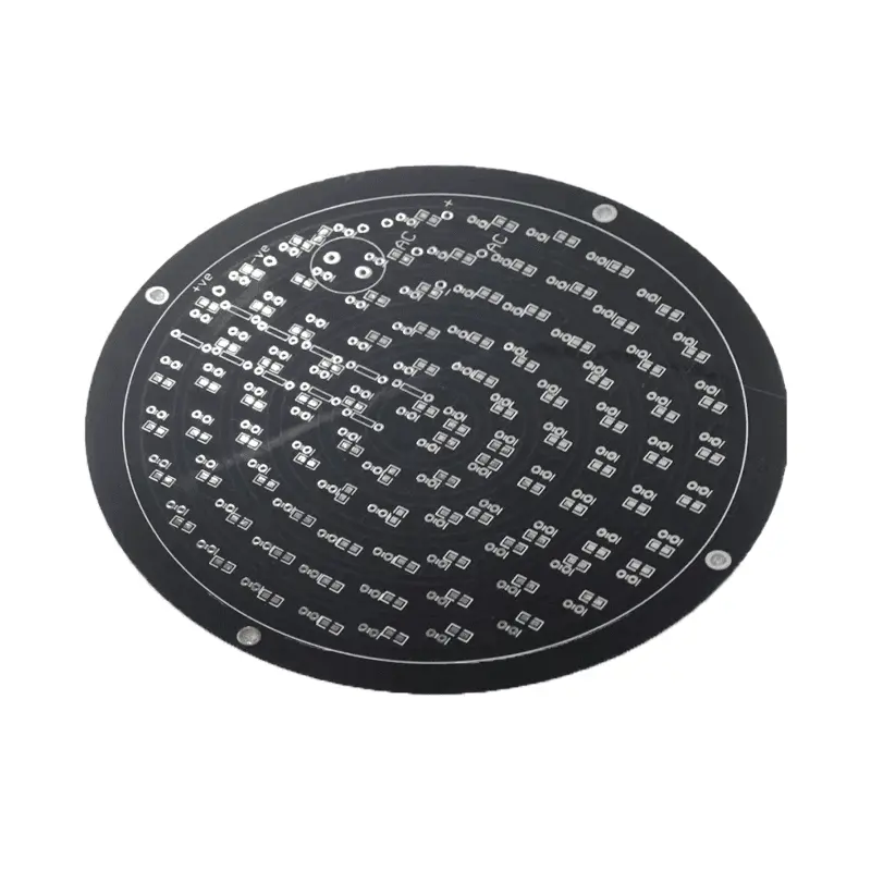
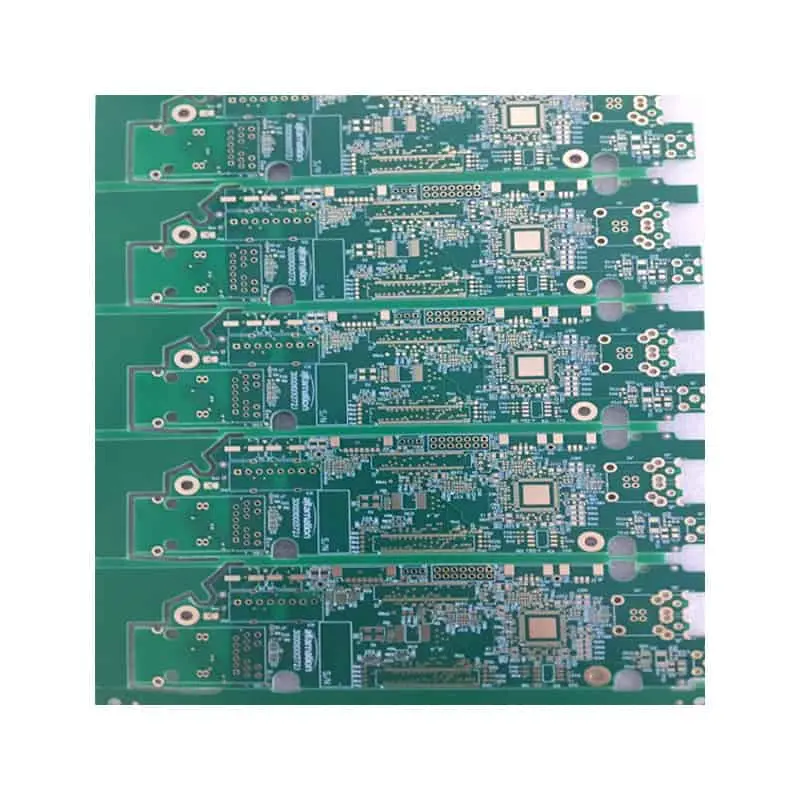
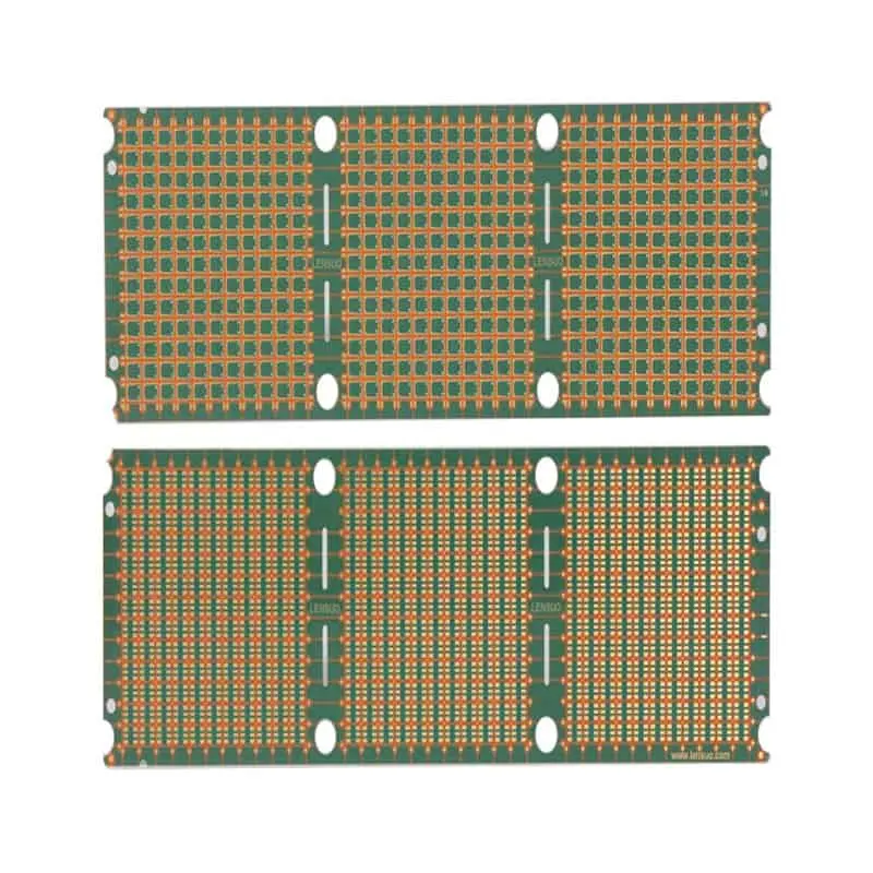
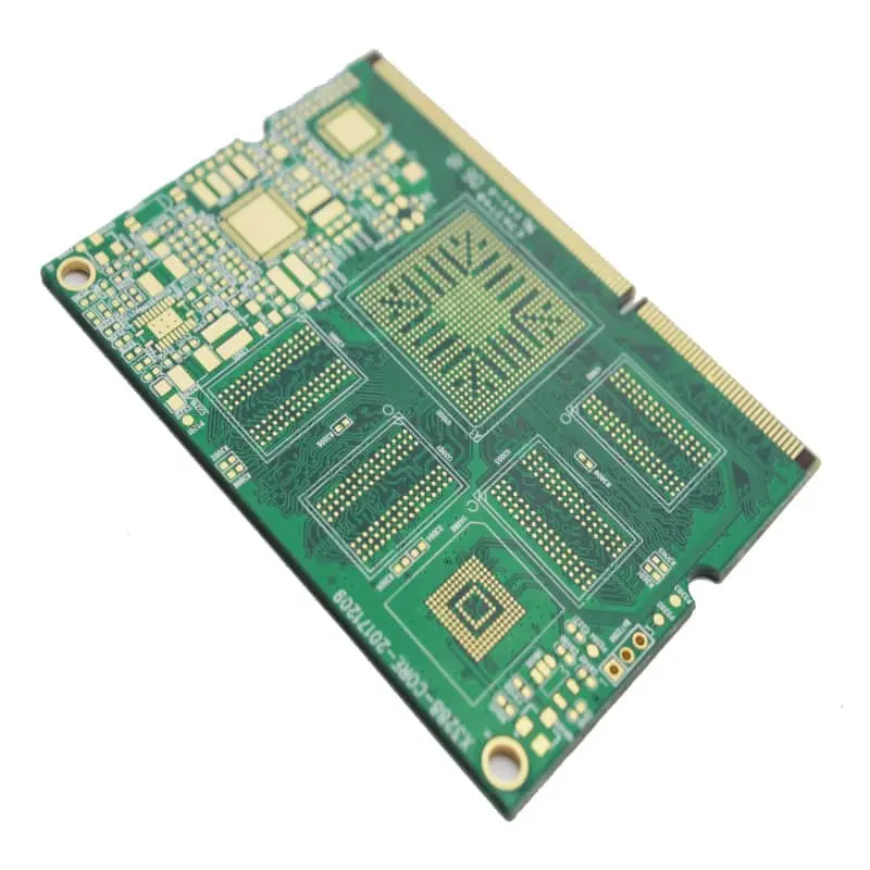
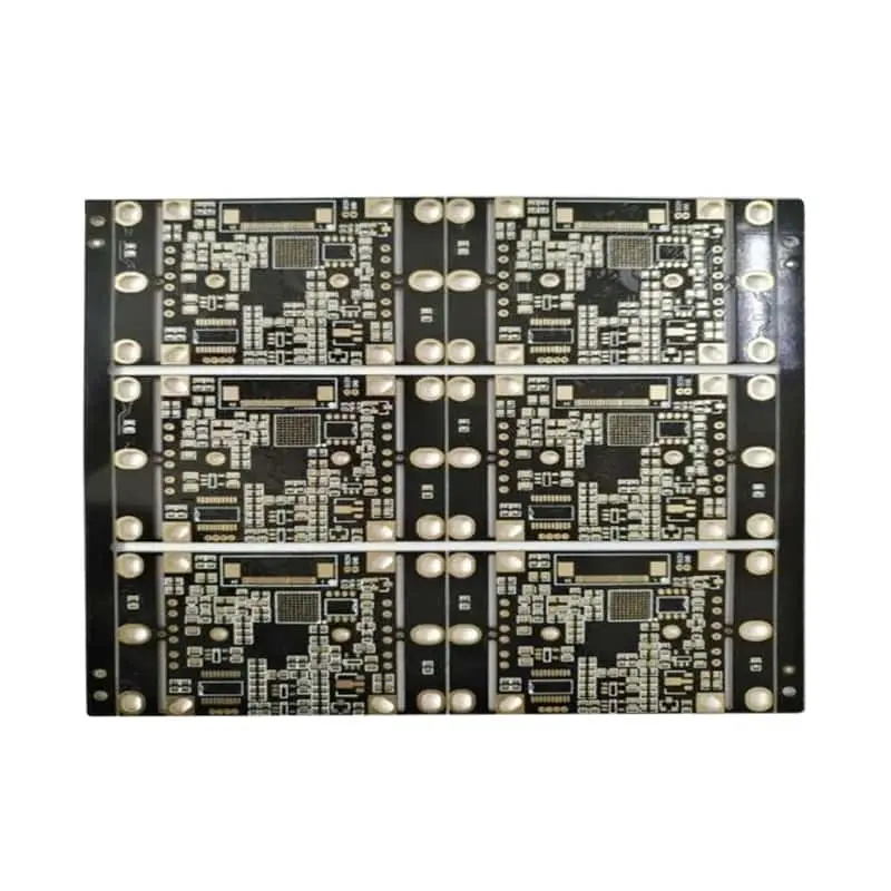
A Multiwire PCB uses insulated conductive wires embedded within a dielectric structure to create point‑to‑point electrical connections. Unlike conventional PCBs that depend mainly on etched copper traces and fixed routing layers, Multiwire technology allows wires to cross within the embedded structure, providing greater routing freedom for specialized high‑density, compact, and complex electronic assemblies.
What Is a Multiwire PCB and How Does It Work?
A Multiwire PCB is a printed circuit board construction that incorporates insulated conductive wires inside a dielectric structure to establish electrical connections between designated points. The embedded wires provide routing paths that are less dependent on conventional copper‑layer geometry and can cross other wires without creating an electrical short because each conductor is individually insulated.
The fundamental difference is how the electrical interconnections are created.
In a conventional multilayer PCB, copper traces are patterned onto individual layers. When a signal needs to move between layers, vias provide the vertical connection. Routing density is therefore strongly influenced by the number of copper layers, trace width and spacing, via dimensions, and available routing channels.
A Multiwire structure takes a different approach. Insulated wires are positioned according to the required electrical connections and subsequently embedded into the board structure. Because the conductors are individually insulated, crossing routes can be implemented without requiring every crossing to occupy a separate copper layer.
A simplified construction can be understood as: Copper circuitry → dielectric material → embedded insulated wires → dielectric material → copper circuitry
The actual construction depends on the selected Multiwire process, materials, electrical requirements, and mechanical design.
Multiwire PCB vs. Conventional PCB Technologies
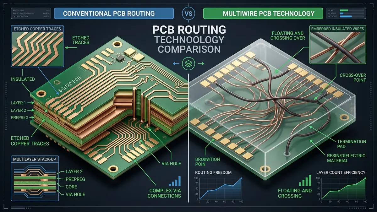
Multiwire PCB vs Conventional PCB Routing Comparison
| Technology | Primary Interconnect | Routing Freedom | Typical Strength |
|---|---|---|---|
| Conventional multilayer PCB | Etched copper traces | Layer‑dependent | Cost‑effective general‑purpose routing |
| HDI PCB | Fine copper traces and microvias | High | Very high routing density |
| Flexible PCB | Etched flexible copper | High | Bendability and compact packaging |
| Multiwire PCB | Embedded insulated wires | Very high for suitable designs | Direct point‑to‑point routing |
The important point is that Multiwire PCB technology should not automatically be treated as a replacement for multilayer, HDI, or flexible PCB technology. Its value appears when its routing architecture solves a particular electrical, packaging, or manufacturing problem more effectively.
What Electrical and Signal Integrity Advantages Does a Multiwire PCB Provide?
A Multiwire PCB can provide shorter and more direct electrical connections while reducing some routing constraints associated with conventional layer‑based PCB design. However, impedance, crosstalk, propagation delay, and signal quality still depend on conductor geometry, dielectric properties, reference structures, operating frequency, and the complete interconnect design.
Routing freedom is one of the most important electrical advantages.
When a conventional PCB becomes heavily congested, engineers may need additional layers, more vias, longer routing paths, or complex layer transitions. A Multiwire architecture can provide alternative point‑to‑point paths that reduce some of these constraints.
Impedance Control
High‑speed signals should not be evaluated simply by looking at conductor resistance.
For a controlled‑impedance interconnect, the electrical behavior depends on factors such as:
- conductor dimensions;
- dielectric constant;
- insulation thickness;
- distance to reference conductors;
- conductor‑to‑conductor spacing;
- operating frequency;
- return‑path geometry.
Common system‑level impedance targets may include 50 Ω single‑ended or approximately 90–100 Ω differential, depending on the interface. These values should be treated as design targets rather than universal Multiwire PCB specifications.
The correct approach is to establish the required impedance from the interface specification and then validate the actual embedded‑wire geometry through field‑solver modeling, TDR, VNA measurement, or another appropriate characterization method.
Crosstalk and Parallel Routing
Crosstalk becomes more important as signal transition times decrease.
The major variables include:
- distance between adjacent conductors;
- length of parallel routing;
- dielectric characteristics;
- conductor geometry;
- reference‑plane arrangement;
- rise/fall time and operating frequency.
Increasing conductor separation generally reduces electromagnetic coupling. Avoiding unnecessarily long parallel runs can also reduce accumulated coupling.
For a high‑speed Multiwire design, engineers should therefore consider the entire coupling environment rather than assuming that insulated wires automatically eliminate crosstalk.
Clock, Differential, and High‑Speed Data Signals
Different signals require different controls.
| Signal Type | Primary Risk | Design Consideration |
|---|---|---|
| Clock | Timing uncertainty | Path‑length and delay control |
| Differential pair | Mode conversion | Symmetry and consistent geometry |
| High‑speed data | Reflection | Controlled impedance |
| Analog signal | Noise coupling | Physical separation and grounding |
| RF signal | Loss and coupling | Controlled geometry and dielectric structure |
The main engineering advantage of Multiwire technology is therefore routing freedom, not a guarantee of superior signal integrity under every operating condition.
What Design Rules and DFM Constraints Apply to Multiwire PCBs?
Multiwire PCB design should define wire diameter, insulation thickness, wire‑to‑wire spacing, clearance from copper features, termination geometry, wire placement tolerance, drilling requirements, and component escape routing before the layout is released for manufacturing.
One of the most common design mistakes is applying conventional PCB terminology too literally.
For a normal copper trace, engineers primarily discuss:
trace width + trace spacing + copper thickness.
For an embedded‑wire structure, the more useful parameters can be:
wire diameter + insulation thickness + center‑to‑center spacing + clearance + termination geometry.
Multiwire PCB Design Parameters
| Parameter | Engineering Question | Manufacturing Impact |
|---|---|---|
| Wire diameter | What conductor size is required? | Routing density and electrical characteristics |
| Insulation thickness | What isolation level and geometry are required? | Effective conductor spacing |
| Wire spacing | How close can adjacent wires run? | Crosstalk and manufacturability |
| Wire placement | How accurately must the wire follow its CAD path? | Electrical and mechanical consistency |
| Termination | How does the embedded wire connect to the PCB? | Connection reliability |
| Component escape | How are dense component pins connected? | Routing complexity |
| Layer position | Where is the wire located within the structure? | Impedance and stack‑up behavior |
| Lamination | How is wire movement controlled? | Dimensional stability |
CAD and DFM Considerations
The CAD database should define the Multiwire geometry explicitly rather than treating embedded wires as an afterthought.
Before releasing the design, the engineering team should verify:
- wire‑to‑wire clearances;
- wire‑to‑pad clearances;
- wire‑to‑hole clearances;
- crossing locations;
- termination areas;
- component keep‑outs;
- drilling and routing features;
- mechanical tolerances;
- assembly access;
- thermal constraints.
A design that works perfectly in a CAD environment may still require modification if the physical wire‑placement process cannot reproduce the intended geometry consistently.
Prototype vs. Production Design
Prototype routing should not automatically be treated as the final production configuration.
During prototyping, engineers may prioritize routing feasibility and electrical validation. Production engineering must additionally consider:
- placement repeatability;
- material availability;
- process capability;
- inspection;
- yield;
- assembly;
- test coverage;
- production throughput.
This is why an early DFM review is particularly valuable for specialized Multiwire PCB designs.
How Is a Multiwire PCB Manufactured and Tested?
Multiwire PCB manufacturing combines conventional PCB materials and fabrication processes with controlled insulated‑wire placement, embedding, lamination, termination, mechanical processing, inspection, and electrical testing.
A simplified manufacturing sequence is: Material Preparation → Wire Placement → Wire Embedding → Lamination → Drilling/Mechanical Processing → Wire Termination → Outer‑Layer Processing → Inspection → Electrical Testing
The actual sequence depends on the manufacturer’s process architecture.
1. Material Preparation
The manufacturer selects the dielectric materials, copper structures, insulated conductors, prepreg or resin systems, and other materials according to the electrical and mechanical requirements.
Material selection affects:
- dielectric behavior;
- thermal expansion;
- mechanical stability;
- lamination behavior;
- signal integrity;
- long‑term reliability.
2. Controlled Wire Placement
The insulated wires are routed according to the engineering data.
At this stage, placement accuracy becomes critical. A wire that is displaced from its intended position can change spacing, coupling, termination geometry, or the electrical characteristics of a high‑speed interconnect.
3. Wire Embedding and Lamination
The wire structure is integrated into the dielectric system.
Lamination requires careful control of:
- temperature;
- pressure;
- resin flow;
- dimensional stability;
- wire movement.
One of the practical manufacturing challenges is maintaining the intended internal geometry while the dielectric material consolidates around the embedded conductors.
4. Drilling and Mechanical Processing
Depending on the construction, drilling, routing, milling, or other mechanical operations may be required to complete component and interconnect features.
The process must avoid damaging embedded conductors and maintain the required dimensional tolerances.
5. Wire Termination
Embedded conductors ultimately need reliable electrical connections to the surrounding PCB circuitry.
Termination is therefore one of the most important reliability interfaces in the entire structure.
6. Inspection and Electrical Testing
A Multiwire PCB should not be qualified solely by visual inspection.
An appropriate inspection program can include:
| Test | Purpose |
|---|---|
| Continuity testing | Verify electrical connections |
| Insulation resistance | Verify conductor isolation |
| Dielectric withstand | Evaluate electrical isolation |
| Cross‑section analysis | Verify internal construction |
| Dimensional inspection | Verify wire placement and geometry |
| Thermal cycling | Evaluate temperature‑related mechanical stress |
| Humidity testing | Evaluate environmental durability |
| Signal‑integrity testing | Validate high‑speed electrical behavior |
The exact acceptance criteria should be established according to the product specification and applicable qualification requirements.
What Are the Main Manufacturing and Reliability Challenges?
The principal Multiwire PCB manufacturing challenges are maintaining wire‑placement accuracy, controlling wire movement during lamination, achieving reliable terminations, inspecting embedded structures, and qualifying the finished board under the application’s thermal, mechanical, electrical, and environmental conditions.
Wire Placement Accuracy
An embedded conductor is not directly visible after the board has been completed.
That creates a fundamental manufacturing challenge: the manufacturer must control the internal geometry before it becomes inaccessible.
Wire Movement During Lamination
Pressure, temperature, and resin flow can affect the position of internal structures.
For this reason, process development should consider not only the nominal CAD position but also the expected manufacturing tolerance.
Termination Reliability
The electrical interface between an embedded wire and the surrounding PCB structure can become a localized reliability concern.
Mechanical stress, thermal expansion, and repeated temperature cycling can affect these interfaces.
Inspection Difficulty
Traditional AOI is highly effective for exposed copper patterns, but embedded conductors require additional verification methods.
Depending on the design, manufacturers may use:
- electrical testing;
- cross‑section analysis;
- dimensional verification;
- specialized internal inspection;
- process‑control records.
Rework
Another practical difference is reworkability.
A conventional exposed copper trace may be relatively accessible. An embedded conductor is inherently less accessible after lamination.
Therefore, design verification before production is especially important for Multiwire assemblies.
Where Are Multiwire PCBs Used and When Are They the Better Choice?
Multiwire PCBs are most attractive when a product requires complex point‑to‑point routing, high interconnect density, compact packaging, or specialized electrical connectivity that is difficult or inefficient to achieve using conventional PCB structures.
Aerospace and Defense
These applications can involve:
- limited installation space;
- complex interconnections;
- high reliability requirements;
- vibration and environmental exposure;
- long product lifecycles.
In such systems, reducing routing complexity or packaging constraints can have system‑level value.
Medical Electronics
Medical equipment can place strong emphasis on:
- compact packaging;
- electrical reliability;
- controlled signal environments;
- repeatable manufacturing;
- long service life.
A Multiwire structure may be considered when conventional routing creates excessive congestion inside a compact assembly.
Telecommunications
Telecommunications equipment can contain a large number of electrical interconnections in restricted physical areas.
Routing freedom can become valuable when conventional layer‑based routing requires excessive layer count or complicated via structures.
Industrial Control
Industrial electronics may prioritize:
- long operating life;
- mechanical robustness;
- predictable manufacturing;
- complex control wiring;
- service reliability.
Multiwire technology can be evaluated when the interconnection architecture itself becomes a packaging constraint.
Specialized Electronics and Legacy Designs
Multiwire technology can also make sense for specialized products where an existing interconnect architecture, mechanical envelope, or point‑to‑point routing requirement makes a conventional PCB redesign unattractive.
However, Multiwire is not automatically the best choice for every high‑density PCB.
How Does Multiwire PCB Compare With Multilayer, HDI, and Flexible PCBs?
Multiwire PCB technology is best viewed as an alternative interconnect architecture rather than a universal replacement for multilayer, HDI, or flexible PCB technology. The correct choice depends on routing density, mechanical requirements, electrical performance, manufacturing capability, volume, and total system cost.
| Factor | Multiwire PCB | Multilayer PCB | HDI PCB | Flexible PCB |
|---|---|---|---|---|
| Routing freedom | Very high for suitable designs | Layer‑dependent | High | High |
| Embedded wiring | Yes | No | No | No |
| Fine‑pitch capability | Application‑dependent | Good | Excellent | Good |
| Mechanical flexibility | Low | Low | Low | High |
| Via dependence | Potentially reduced | High | High | Medium |
| Manufacturing availability | More specialized | Very high | High | High |
| Prototype economics | Application‑dependent | Generally favorable | Application‑dependent | Application‑dependent |
| Primary advantage | Point‑to‑point routing freedom | General‑purpose complexity | High‑density miniaturization | Bendable packaging |
The engineering decision should therefore start with the actual problem.
If the primary problem is fine‑pitch component escape, HDI may be more appropriate.
If the primary problem is mechanical bending, flexible PCB may be the natural solution.
If the requirement is general multilayer routing at competitive volume cost, conventional multilayer PCB may remain the better choice.
If the challenge is specialized point‑to‑point routing within a dense or constrained structure, Multiwire deserves evaluation.
Does a Multiwire PCB Cost More Than a Conventional PCB?
A Multiwire PCB can have higher specialized manufacturing or setup costs than a conventional PCB, but total project economics depend on routing complexity, board size, layer count, production volume, engineering effort, prototype iterations, testing, and lifecycle requirements.
A meaningful cost comparison should therefore consider total cost of ownership, rather than PCB unit price alone.
A practical TCO model is: Total Cost of Ownership = Fabrication + Engineering + Prototype Iterations + Assembly + Testing + Qualification + Lifecycle Costs
For a prototype, the engineering and setup portion may represent a significant share of total cost.
For high‑volume production, unit manufacturing economics become increasingly important.
This creates an important decision point:
A technology that saves engineering time or eliminates routing complexity is not automatically cheaper on a per‑board basis.
The correct question is:
Does Multiwire reduce the total cost or technical risk of the complete product?
That is the basis for a meaningful ROI analysis.
What Should You Ask a Multiwire PCB Manufacturer Before Ordering?
Before placing a Multiwire PCB order, procurement and engineering teams should confirm the manufacturer’s wire‑placement capability, supported materials, termination technology, inspection methods, electrical testing, DFM process, prototype support, and production qualification requirements.
A supplier evaluation should include at least the following questions:
- What wire diameters and insulated conductor structures can you manufacture?
- What wire‑placement tolerance can you qualify for production?
- What dielectric and PCB material systems are supported?
- How is wire displacement controlled during embedding and lamination?
- How are embedded wires inspected after manufacturing?
- What continuity and insulation tests are available?
- Can you provide cross‑section or qualification reports?
- What information is required for a DFM review?
- What prototype quantities and production volumes can you support?
- How are engineering changes handled between prototype and mass production?
A qualified supplier should be able to discuss these questions in engineering terms rather than simply provide a unit price.
How Can You Request a Multiwire PCB Engineering Review?
A Multiwire PCB feasibility review should begin with the electrical requirements, CAD or routing information, mechanical constraints, material requirements, production quantity, and applicable testing or qualification standards.
For an initial evaluation, provide as much of the following information as available:
- PCB drawings;
- Gerber or CAD files;
- preliminary stack‑up;
- wire requirements;
- component information;
- operating frequency;
- impedance targets;
- mechanical dimensions;
- quantity;
- prototype requirements;
- environmental requirements;
- applicable quality or qualification standards.
The engineering review can then focus on: Routing feasibility → Wire geometry → DFM → Signal integrity → Manufacturing process → Testing → Prototype → Production
For complex designs, resolving manufacturability issues before fabrication is usually more valuable than discovering them after the first prototype has been built.
Need to determine whether Multiwire is suitable for your design? Submit your PCB requirements to Shenzhen Haoda Circuit Technology Co., Ltd. for an engineering feasibility and DFM review.
Request a Multiwire PCB Engineering Review → Email:pcb@pcbcoming.com
Frequently Asked Questions
What industries and applications benefit most from Multiwire PCBs?
Aerospace, defense, medical electronics, telecommunications, industrial controls, and other specialized electronic systems can benefit when routing density, packaging constraints, or complex point-to-point interconnections make conventional PCB routing difficult.
How does a Multiwire PCB compare with a conventional multilayer or HDI PCB?
Multiwire uses insulated embedded conductors to provide routing freedom, while conventional multilayer and HDI PCBs primarily use etched copper traces and vias. HDI is often preferable for fine-pitch and miniaturized designs, whereas Multiwire can be attractive for specialized point-to-point routing requirements.
What design rules should engineers consider when designing a Multiwire PCB?
Engineers should define wire diameter, insulation thickness, wire spacing, clearance, termination geometry, placement tolerance, component escape routing, drilling requirements, and electrical targets before releasing the design for manufacturing.
How are embedded wires inspected and tested during Multiwire PCB manufacturing?
Depending on the construction and qualification plan, inspection can include dimensional verification, cross-section analysis, continuity testing, insulation resistance, dielectric withstand, environmental testing, and signal-integrity characterization.
What information should I provide when requesting a Multiwire PCB quote?
Provide the PCB drawings or CAD/Gerber files, dimensions, quantity, wire requirements, material requirements, electrical specifications, impedance targets, component information, testing requirements, and applicable industry or customer standards. The more complete the engineering information, the more accurately a supplier can evaluate feasibility, cost, and lead time.
Engineering Takeaway
Multiwire PCB technology should not be selected simply because it offers greater routing freedom. The better engineering approach is to compare the complete interconnect architecture against conventional multilayer, HDI, and flexible PCB alternatives.
For the right application, embedded insulated wiring can simplify difficult point-to-point routing and create packaging options that are difficult to achieve with conventional layer-based routing. For other applications, conventional PCB technologies may provide better availability, cost, or manufacturing scalability.
The most reliable selection process is therefore:
Define the electrical problem → evaluate routing constraints → compare technologies → perform DFM → validate the construction → prototype → qualify → release for production.
For specialized Multiwire PCB requirements, early collaboration between the PCB designer, signal-integrity engineer, manufacturer, and procurement team can prevent expensive redesigns and qualification delays.
About Author
David Chen https://www.linkedin.com/in/pcbcoming
David Chen boasts an extensive professional background in PCBA manufacturing, PCBA testing, and PCBA optimization, with specialized expertise in high-precision PCBA fault analysis and rigorous PCBA reliability testing. The author has worked with high-layer-count server PCB fabrication, ultra-low-loss backplane stackups, and thermo-mechanical reliability optimization for AI infrastructure projects involving 112G and 224G PAM4 architectures. Skilled in complex circuit design and cutting-edge advanced PCB manufacturing processes, he delivers solutions that elevate product durability and performance across industrial applications. His technical articles focusing on PCBA manufacturing workflows and testing methodologies are widely cited by industry peers, research institutions, and technical platforms, solidifying his reputation as a recognized technical authority in the global circuit board manufacturing sector.