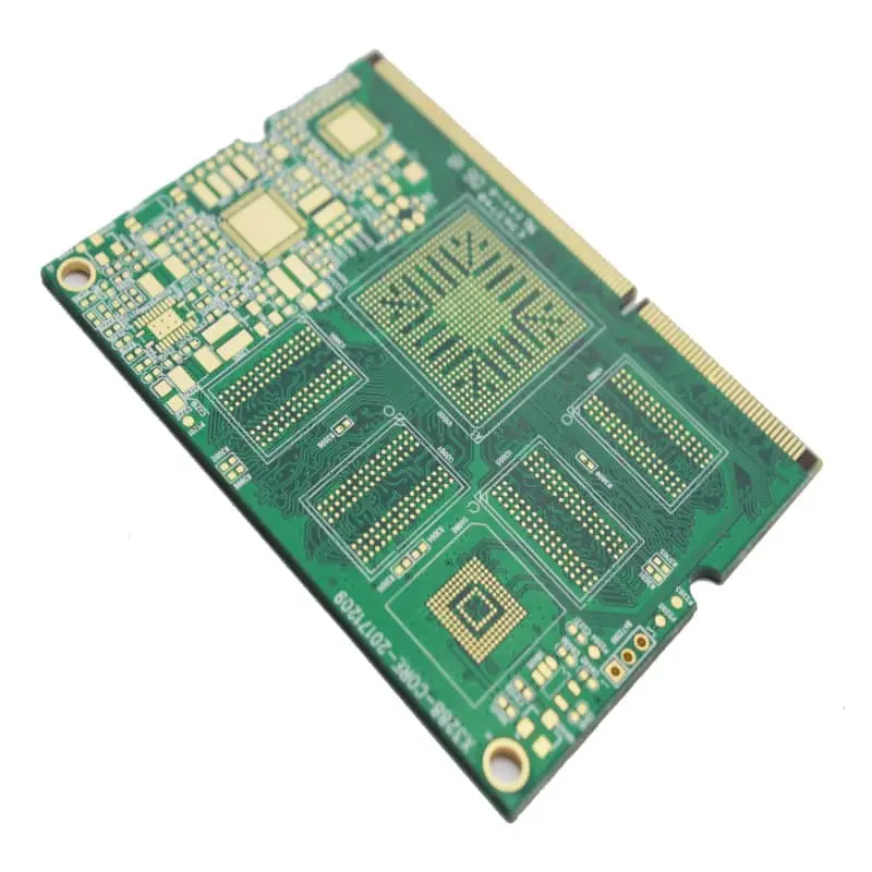
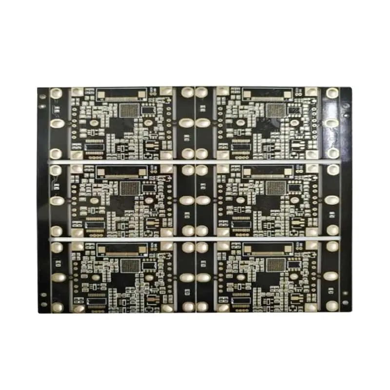
Choosing the correct Rogers 5880 thickness is not simply a mechanical decision. For RF, microwave, antenna, radar, satellite, and high-frequency communication PCBs, dielectric thickness directly affects impedance, trace geometry, insertion loss, board stiffness, multilayer construction, drilling, fabrication yield, and ultimately the cost of the finished PCB.
Rogers RT/duroid 5880 is a glass microfiber-reinforced PTFE laminate designed for demanding microstrip and stripline applications. Rogers specifies a process dielectric constant of 2.20 ± 0.02 and a typical dissipation factor of 0.0009 at 10 GHz.
For procurement, the correct specification should therefore include more than “Rogers 5880.” The RF PCB supplier should receive the required dielectric thickness, thickness tolerance, copper type, copper weight, finished board thickness, stack-up, impedance requirement, and surface finish.
Available Rogers 5880 Thicknesses and Standard Panel Sizes
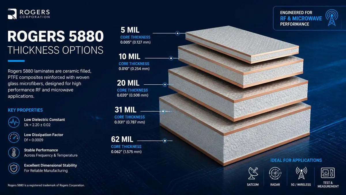
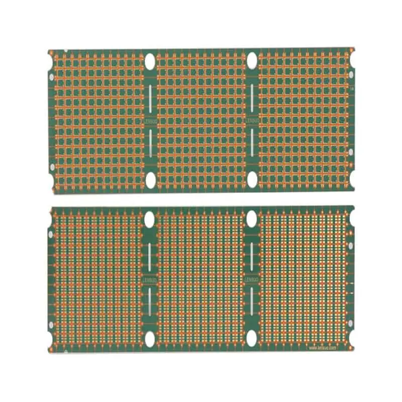
Rogers 5880 Thickness Options and Core Stack-Up Chart
Rogers currently lists five standard RT/duroid 5880 laminate thicknesses, while additional thicknesses are available from 0.0035 in to 0.375 in in varying increments.
| Nominal Thickness | Approx. mm | Thickness Tolerance | Typical Procurement Description |
|---|---|---|---|
| 5 mil | 0.127 mm | ±0.0005 in / ±0.0127 mm | RT/duroid 5880, 5 mil |
| 10 mil | 0.252 mm | ±0.0007 in / ±0.0178 mm | RT/duroid 5880, 10 mil |
| 20 mil | 0.508 mm | ±0.0015 in / ±0.0381 mm | RT/duroid 5880, 20 mil |
| 31 mil | 0.787 mm | ±0.0020 in / ±0.0508 mm | RT/duroid 5880, 31 mil |
| 62 mil | 1.575 mm | ±0.0030 in / ±0.0762 mm | RT/duroid 5880, 62 mil |
The published standard panel sizes are 18 × 12 in (457 × 305 mm) and 18 × 24 in (457 × 610 mm), with additional panel sizes available.
A critical procurement point is that the Rogers datasheet does not present these products as a simple public list of individual SKU numbers. Instead, Rogers states that buyers should specify the dielectric thickness and tolerance together with the copper construction.
For example, a purchasing specification should read more like:
RT/duroid 5880, 10 mil dielectric, specified thickness tolerance, 1 oz copper, ED or rolled copper as required, finished PCB according to supplied Gerber and stack-up.
This prevents a common purchasing error: treating “5880” as a complete material specification when the copper construction and dielectric thickness have not actually been defined.
Electrical Performance: Dk, Df and Impedance by Thickness
The principal reason engineers select Rogers 5880 is its stable low-loss electrical behavior. Rogers specifies a process Dk of 2.20 ± 0.02, a typical design Dk of 2.20, and a typical dissipation factor of 0.0009 at 10 GHz.
| Electrical Property | RT/duroid 5880 |
|---|---|
| Process Dk | 2.20 ± 0.02 |
| Design Dk | 2.20 |
| Dissipation factor at 10 GHz | 0.0009 typical |
| Volume resistivity | 2 × 10⁷ MΩ·cm |
| Surface resistivity | 3 × 10⁷ MΩ |
| Water absorption | 0.02% typical |
| Thermal conductivity | 0.20 W/m/K typical |
The important engineering distinction is that laminate thickness does not simply change the intrinsic Dk of RT/duroid 5880. Instead, thickness changes the electromagnetic geometry of the transmission line.
For a microstrip, increasing dielectric thickness generally requires a wider trace to maintain the same characteristic impedance. Reducing dielectric thickness normally requires a narrower trace. The exact width also depends on copper thickness, trace etch profile, solder mask, Dk, and the geometry of the surrounding reference plane.
For a 50 Ω design, engineers should therefore avoid specifying a generic trace width such as “8 mil for 50 Ω.” The correct width must be calculated from the actual stack-up.
Rogers specifically notes that the reported process Dk and tolerance values are used for quality acceptance, while design Dk can be more appropriate for certain design situations. Rogers also recommends verifying prototype boards for the desired electrical performance, particularly for new designs.
For production RF PCB procurement, the recommended workflow is:
- Define the required impedance, such as 50 Ω single-ended or 100 Ω differential.
- Select the Rogers 5880 dielectric thickness.
- Define copper weight and copper type.
- Build the complete stack-up.
- Calculate trace width and spacing.
- Account for fabrication tolerances.
- Validate the first article with impedance testing.
This is more reliable than selecting a Rogers 5880 thickness based only on the nominal board thickness.
Mechanical and Thermal Behavior: Flexibility, Stiffness and Stack-Up Guidance
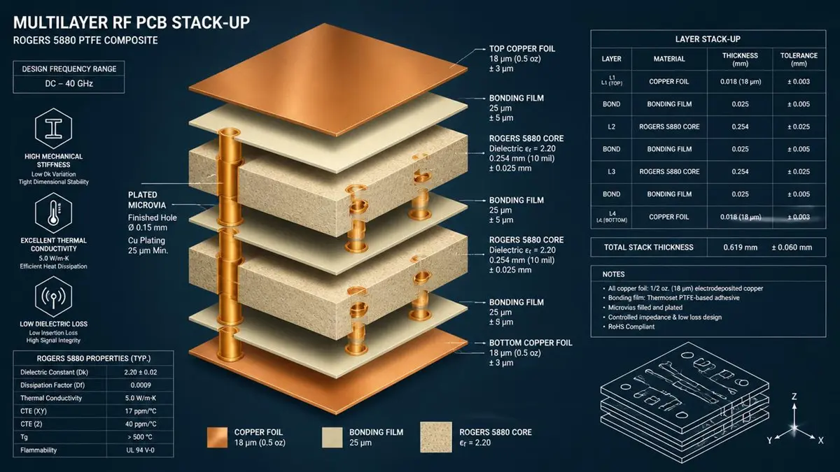
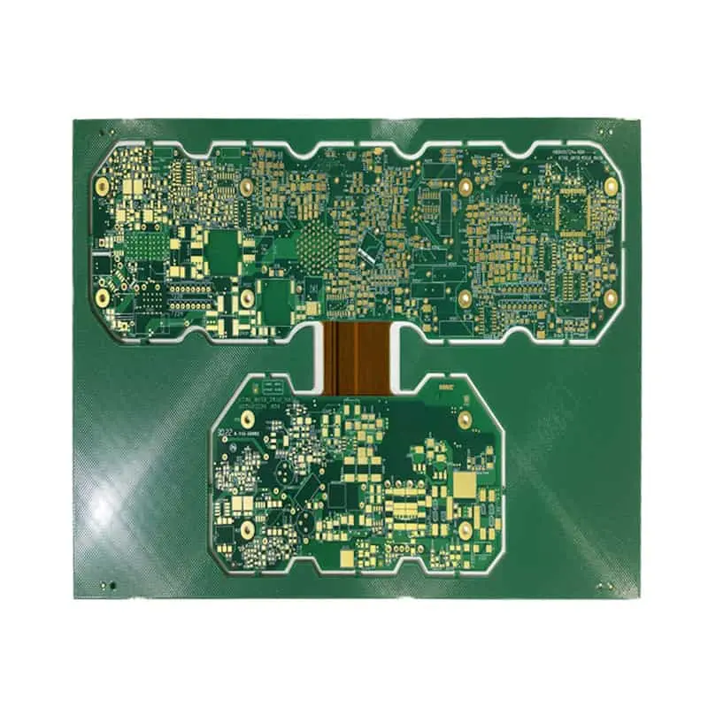
Rogers 5880 Multilayer RF PCB Stack-Up and Layer Structure Diagram
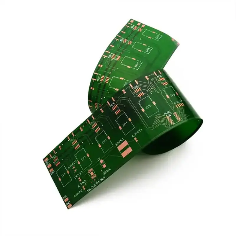
Rogers 5880 is a PTFE-based material and is mechanically softer than conventional rigid epoxy-glass laminates. Rogers’ fabrication guideline specifically warns that PTFE-based materials are more susceptible to handling damage and that thin copper-clad cores can be creased.
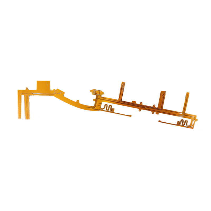
From a mechanical standpoint, increasing dielectric thickness increases bending stiffness significantly. This is why very thin 5 mil and 10 mil constructions are useful when compact RF geometries or controlled transmission-line spacing are required, while 31 mil and 62 mil materials may be more appropriate when mechanical rigidity or a larger RF dielectric spacing is required.
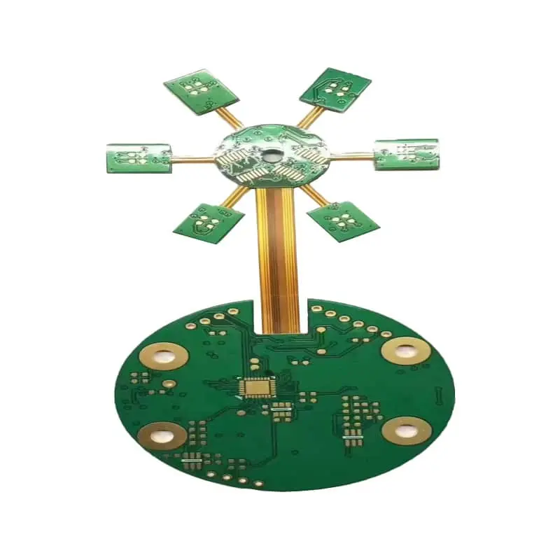
For multilayer RF PCBs, thickness should be selected together with the complete stack-up rather than independently.
A practical stack-up definition should identify:
- Core dielectric thickness
- Bonding-film thickness
- Copper thickness before and after plating
- Signal and reference-plane layers
- Finished board thickness
- Controlled-impedance layers
- Via structure
- Surface finish
Rogers permits thermoplastic and thermoset bonding systems for multilayer constructions. For electrically critical applications, thermoplastic systems such as FEP or Rogers 3001 film can be selected; thermoset systems can be considered where adhesive electrical properties are less critical.
For FEP bonding, Rogers specifies a bonding temperature range of approximately 275–290°C with controlled pressure and cooling. Cooling should remain under pressure because transfer cooling can contribute to delamination.
This is particularly important when combining thin and thick Rogers layers. A supplier should calculate the cumulative stack-up tolerance rather than simply adding nominal dielectric values.
Copper Cladding, Surface Finishes, Fabrication and Handling Best Practices
Rogers 5880 can be supplied with electrodeposited copper, reverse-treated EDC, or rolled copper foil for more demanding electrical applications. The standard datasheet lists ½ oz (18 µm) and 1 oz (35 µm) configurations, while the material can generally be supplied with copper cladding from approximately 8 to 70 µm depending on configuration.
Rolled copper can be particularly relevant when conductor surface characteristics are important to RF loss. Copper roughness becomes increasingly important as frequency rises because current distribution shifts toward the conductor surface.
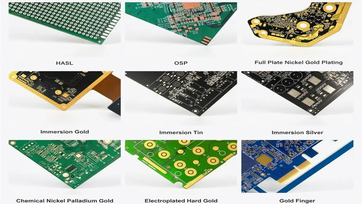
For PCB fabrication, surface preparation also matters. Rogers states that conventional final metal surfaces such as HASL, tin, Sn/Pb, nickel/gold, silver and OSP can be applied using normal procedures.
However, the fabrication process itself requires more control than standard FR-4 processing.
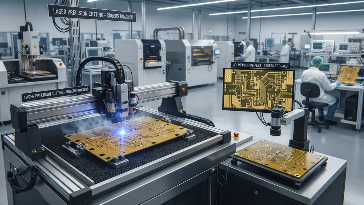
Rogers recommends carbide drills and conservative drilling conditions. Its fabrication guideline specifies approximately 150–250 SFM and 0.0015–0.0025 in/rev as recommended drilling parameters, with controlled tool life.
For routing, carbide double-fluted spiral-up end mills are preferred. Rogers recommends approximately 150 SFM and a lateral feed of 0.002 in/rev, with an estimated tool life of 30–50 feet of linear travel.
Storage and handling should also be controlled. Thin panels should remain protected in their packaging, while panels should be supported properly to prevent creasing or dimensional distortion.
Pricing, Lead Times, Part Numbers, Distributors and Alternatives
Rogers 5880 pricing is not determined by dielectric thickness alone. A production RF PCB quotation normally depends on:
- Laminate thickness
- Copper type and weight
- Panel size
- Number of layers
- Finished PCB dimensions
- Minimum trace/space
- Controlled impedance requirements
- Hole sizes and via structure
- Surface finish
- Quantity
- Prototype versus production volume
- Material availability
Because Rogers does not publish a universal public price list for every thickness and configuration, a supplier should confirm current material availability and quotation before the purchase order is released.
The same principle applies to part numbers. Rather than inventing a generic “Rogers 5880 SKU,” procurement teams should specify the material configuration directly and request the supplier to confirm the manufacturer’s exact material identification and lot traceability.
Rogers states that each panel is labeled with product identification, lot and sheet numbers, and that traceability is maintained based on these identifiers.
Rogers 5880 vs. RO4350B
| Requirement | RT/duroid 5880 | RO4350B |
|---|---|---|
| Material family | PTFE composite | Hydrocarbon/ceramic |
| Typical Dk | 2.20 | Higher |
| Low-loss RF | Excellent | Very good |
| RF/microwave antennas | Excellent fit | Good fit |
| Fabrication complexity | Higher | Generally easier |
| Cost optimization | Application dependent | Often attractive |
| Typical use | Microwave, radar, antennas | RF, power amplifiers, wireless |
The best alternative depends on the application rather than simply the material price.
If the design requires the very low loss and low Dk associated with PTFE-based microwave construction, RT/duroid 5880 remains an appropriate candidate. If easier conventional PCB processing, higher mechanical robustness, or cost optimization is more important, an RO4000-series material such as RO4350B may deserve evaluation.
Request a Rogers 5880 PCB Quote by Thickness
For engineers and procurement teams, the fastest way to obtain an accurate Rogers 5880 PCB quotation is to provide the complete material configuration rather than only specifying “Rogers 5880.”
Include:
Rogers 5880 + dielectric thickness + thickness tolerance + copper type + copper weight + layer count + finished board thickness + impedance requirement + surface finish + quantity.
For example:
Material: RT/duroid 5880
Dielectric: 10 mil
Copper: 1 oz ED copper
Impedance: 50 Ω controlled
Surface finish: ENIG
Quantity: 10 prototypes / 500 production units
A PCB manufacturer can then verify material availability, stack-up feasibility, impedance geometry, fabrication tolerances, lead time, and production cost before the order is released.
For new RF designs, the most useful procurement package should include the Gerber files, drill files, stack-up drawing, impedance requirements, material specification, copper weight, surface finish, and controlled-impedance test requirements.
FAQ
What are the standard thicknesses available for Rogers 5880?
The standard RT/duroid 5880 thicknesses listed by Rogers are 5 mil, 10 mil, 20 mil, 31 mil and 62 mil. Additional thicknesses from approximately 3.5 mil to 375 mil are available in varying increments.
How does Rogers 5880 Dk and Df vary with frequency and board thickness?
Rogers specifies a process Dk of 2.20 ± 0.02 and a typical design Dk of 2.20. The typical dissipation factor is 0.0009 at 10 GHz. Thickness changes the transmission-line geometry and therefore the resulting impedance and loss, but it should not be treated as a simple change to the material’s intrinsic Dk.
Which Rogers 5880 thickness is best for a 50 Ω microstrip?
There is no universal thickness that produces 50 Ω. The correct choice depends on dielectric thickness, copper thickness, trace width, trace spacing, reference-plane location, Dk and fabrication tolerances. The complete stack-up should be calculated before PCB fabrication.
What copper foil options are available?
Rogers lists standard ½ oz (18 µm) and 1 oz (35 µm) electrodeposited copper and corresponding rolled-copper options. Other copper configurations can also be available depending on the product configuration.
Where can I find the manufacturer data for each Rogers 5880 thickness?
Rogers provides the official RT/duroid 5870/5880 datasheet, fabrication guidelines, laminate properties tool and electrical-design resources. The manufacturer’s documentation should be treated as the primary reference when confirming material properties and ordering configurations.
How does Rogers 5880 compare with RO4350B?
Rogers 5880 is a PTFE-based low-loss material optimized for demanding microwave and high-frequency applications. RO4350B belongs to the RO4000 family and uses a different material system that can offer a different balance between RF performance, manufacturability, mechanical behavior and cost. The correct choice should be based on the required electrical and manufacturing performance rather than material price alone.
Final Procurement Checklist
Before placing a Rogers 5880 PCB order, confirm these eight items:
- Exact dielectric thickness
- Thickness tolerance
- Copper type: ED, reverse-treated or rolled
- Copper weight
- Layer stack-up and finished thickness
- Controlled impedance requirement
- Surface finish
- Quantity and delivery requirement
For RF and microwave PCB production, thickness selection should be treated as part of the electrical design—not as a standalone purchasing parameter. A properly specified Rogers 5880 construction gives the PCB manufacturer enough information to validate impedance, fabrication capability, material availability and production cost before manufacturing begins.
For a project-specific quotation, submit the required Rogers 5880 thickness, copper weight, layer count, board dimensions, Gerber files and impedance requirements for engineering review and procurement confirmation.
David Chen LinkedIn Profil
David Chen is a Senior RF/PCB Process Engineer at Shenzhen Haoda Circuit Technology Co., Ltd., with over 12 years of experience in high-frequency PCB fabrication, impedance-controlled stack-up design, and Rogers/PTFE laminate processing. He also boasts an extensive professional background in PCBA manufacturing, PCBA testing, and PCBA optimization, with specialized expertise in high-precision PCBA fault analysis and rigorous PCBA reliability testing. The author has worked with high-layer-count server PCB fabrication, ultra-low-loss backplane stackups, and thermo-mechanical reliability optimization for AI infrastructure projects involving 112G and 224G PAM4 architectures. Skilled in complex circuit design and cutting-edge advanced PCB manufacturing processes, he delivers solutions that elevate product durability and performance across industrial applications. His technical articles focusing on PCBA manufacturing workflows and testing methodologies are widely cited by industry peers and technical platforms, and have gained attention and recognition from industry colleagues.