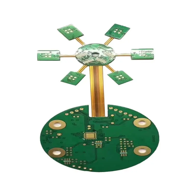
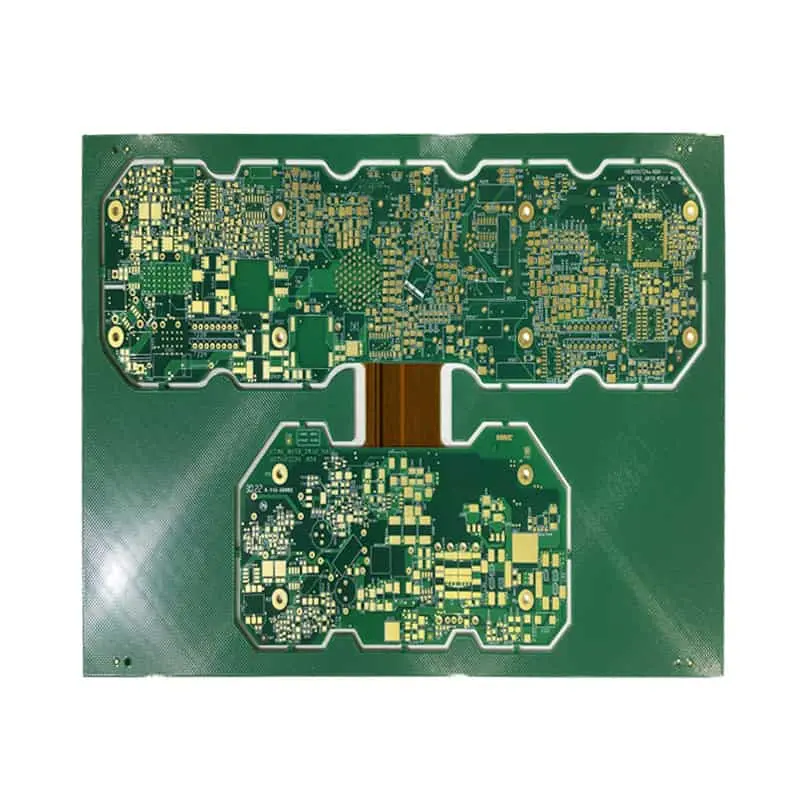
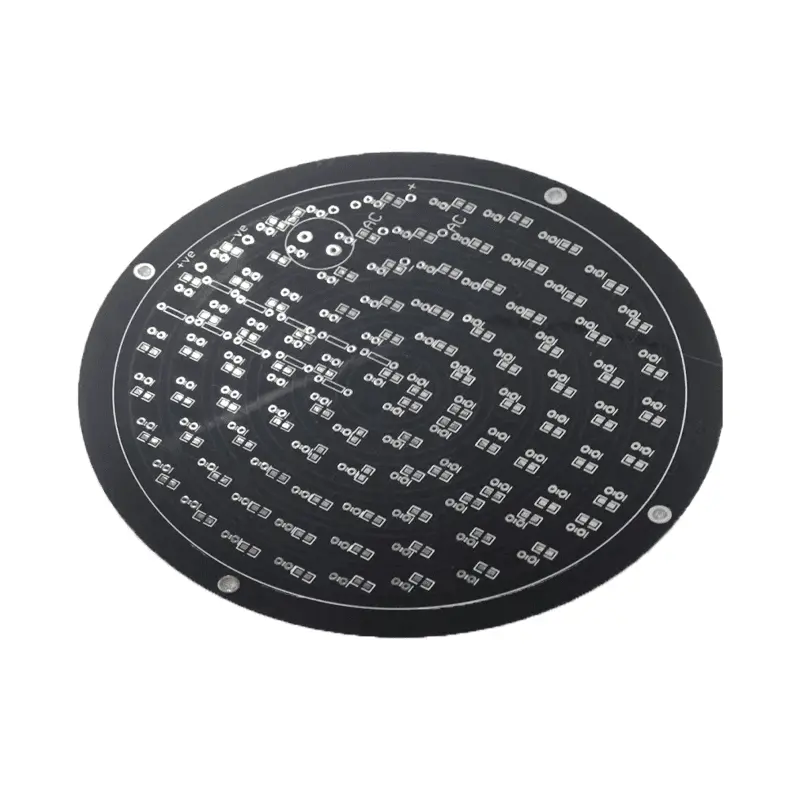
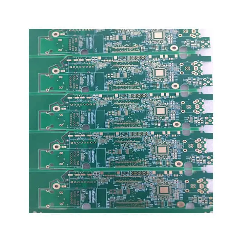
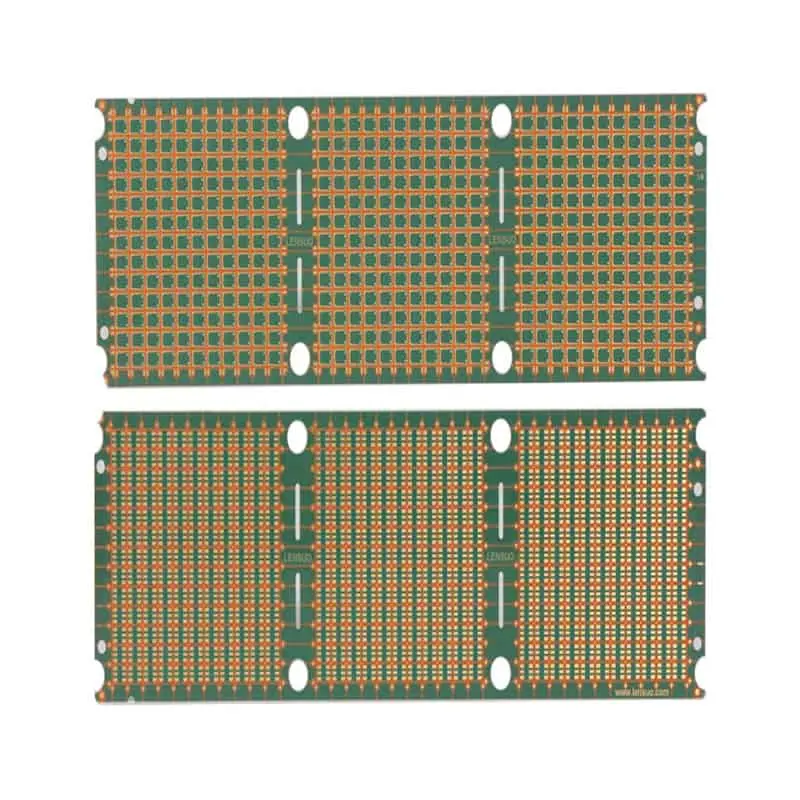
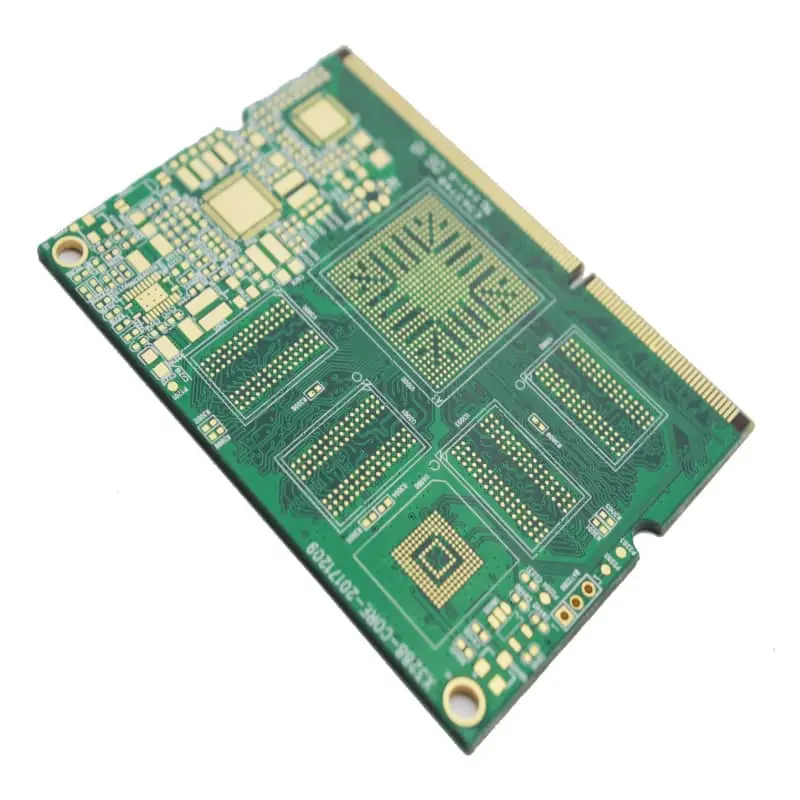
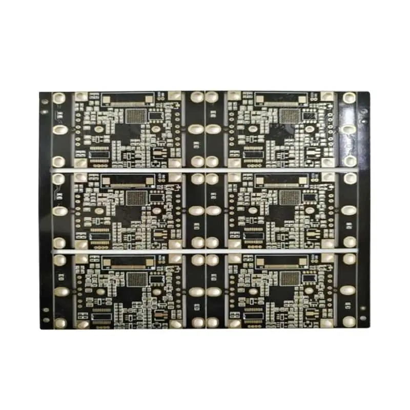
Rogers RO4350B high frequency PCB manufacturer selection is critical because Rogers RO4350B is one of the most widely specified hydrocarbon ceramic laminates for RF and microwave designs — from 5G infrastructure and radar to aerospace telemetry and test instrumentation. Unlike standard FR-4, RO4350B delivers stable dielectric performance across multi-GHz frequencies, but that performance only materializes when the right manufacturer, the right stackup, and the right test plan are in place. This guide consolidates everything procurement teams and RF engineers need to evaluate, specify, and buy RO4350B boards with confidence.
1: Verified Rogers RO4350B PCB Manufacturers (U.S. and Recommended Global Partners)
For the U.S. market, the following manufacturers have documented, production-level experience with RO4350B:
- U.S.-based fabrication partners — Fabricators with domestic facilities (e.g., in California, Texas, Arizona, and New England) typically offer prototype lead times of 3–5 business days and production runs of 2–4 weeks, with MOQs as low as 1–5 panels for prototypes. Look for IPC-6012 Class 2/3 certification and ITAR-registered facilities for defense work.
- Offshore high-mix specialists — Vetted Asian partners with dedicated RF lines (many serving U.S. customers through U.S. sales offices) offer 24–72 hour quick-turn prototypes and 5–10 day production, often at 30–50% lower cost, with DHL/FedEx door-to-door delivery in 2–3 days to U.S. addresses.
- Quick-turn RF specialists — A subset of U.S. shops focuses exclusively on RF prototypes, offering same-week delivery on 2-layer and 4-layer RO4350B boards with TDR reports included.
What to verify before requesting a quote: actual Rogers laminate certificates of conformance (CoC) — not generic “ceramic-filled PTFE” substitutes; recent TDR/VNA test report samples; impedance-controlled process capability (Cpk data if available); and AS9100/ISO 9001 certification for aerospace programs.
Vetting checklist and quote-preparation essentials:
- Demand laminate lot traceability and Rogers CoC documentation.
- Provide complete Gerber (RS-274X), drill files, IPC netlist, and stackup drawing with impedance tables.
- Specify board outline with dimensional tolerances and controlled-depth routing requirements.
- State test requirements up front: coupon TDR, 100% netlist electrical test, and S-parameter verification if needed.
- Confirm panelization and scoring/routing preferences, plus any serialization or UL marking requirements.
2: RO4350B Electrical, Dielectric and Thermal Properties (Frequency-Dependent Datasheet Highlights)
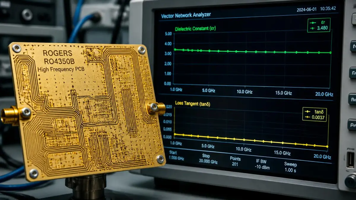
Rogers RO4350B high frequency PCB manufacturer Dielectric and Loss Test
The reason engineers select RO4350B over FR-4 is its frequency stability. Key Rogers-published values:
| Parameter | Value | Conditions |
|---|---|---|
| Dielectric constant (Dk / εr) | 3.48 ± 0.05 | 10 GHz, 23°C (process design Dk ~3.66 for impedancing) |
| Loss tangent (Df / tanδ) | 0.0037 | 10 GHz |
| Df | 0.0031 | 2.5 GHz |
| Thermal conductivity | 0.69 W/m·K | Through-plane |
| CTE (x, y) | ~10–12 ppm/°C | In-plane, near copper match |
| CTE (z-axis) | ~35 ppm/°C | Below Tg (~280°C decomposition threshold) |
| Copper peel strength | ~1.0–1.4 N/mm | After solder float |
Engineering implications:
- Impedance control: Because εr barely drifts from 1 GHz to 10+ GHz (unlike FR-4, which can vary 5–10%), a stackup designed at 3.66 stays predictable in production. Specify the manufacturer’s process Dk, not the nominal 3.48, when calculating line widths.
- Loss budgeting: At Df ≈ 0.0037–0.004, expect roughly 0.3–0.5 dB per inch insertion loss at 10 GHz for a 50Ω microstrip on 20 mil core, depending on copper roughness. At mmWave (28–39 GHz), budget 1.0–1.5 dB/inch — this is where smooth/very-low-profile copper (HVLP) becomes critical.
- Thermal management: 0.69 W/m·K is far better than FR-4 (~0.3 W/m·K) but still modest for power amplifiers. Plan thermal via stitching, embedded copper coins, or heavier copper for >5 W dissipation channels.
- Reliability: Tg >280°C and matched in-plane CTE enable lead-free reflow without via barrel cracking — a common FR-4 failure mode in RF assemblies.
3: Fabrication Capabilities, Tolerances and RF Testing for RO4350B Boards
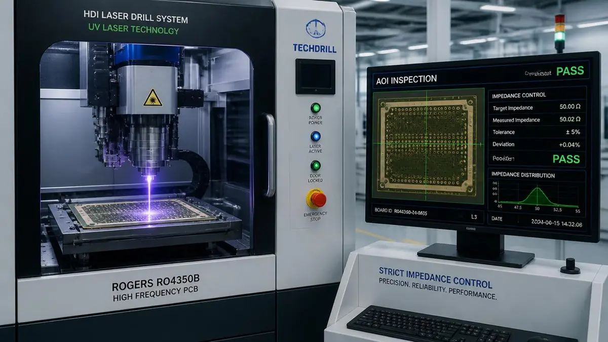
Rogers RO4350B high frequency PCB manufacturer Laser Drilling and AOI Inspection
Specify these values directly in your fabrication notes and purchase orders:
Impedance control
- Single-ended and differential: ±5% achievable on controlled layers (±10% standard). Always request statistical TDR data on impedance coupons, not just pass/fail statements.
Dimensional capability
- Minimum trace/space: 3/3 mil (production-proven); 4/4 mil recommended for yield on volume.
- Minimum drilled hole: 0.15 mm (6 mil) mechanical; laser microvias from 4 mil.
- Hole registration / annular ring: ±2 mil; controlled-depth drilling for cavity or via-in-pad applications to ±3 mil depth tolerance.
- Copper thickness: 0.5 oz to 2 oz outer; 1 oz standard for inner RF reference planes. Heavy copper (3–4 oz) available with reduced etch tolerance.
- Board thickness: 8 mil to 120 mil overall; RO4350B cores available in 4, 6.6, 8, 10, 13.3, 16.6, 20, 30, 60 mil.
Lamination & drilling guidance
- Laminate per Rogers recommendations: typical press cycle 185–200°C, 350–450 psi, 60–90 minutes cure, with controlled ramp rates (≤3°C/min) to prevent resin starvation or voids.
- Use new, sharp carbide drill bits at high RPM with entry/exit backing material; RO4350B drills cleanly but smear control matters for plated through-hole quality.
Surface finishes and RF impact
- ENIG: best planarity and shelf life; negligible RF impact — recommended for fine-pitch RF components.
- Immersion silver: excellent high-frequency performance (low skin-effect resistance), but requires nitrogen storage and prompt assembly.
- OSP: good for RF, limited shelf life.
- Avoid HASL for high-frequency boards — non-planar surface degrades launch geometry and repeatability.
Testing you should require
- TDR impedance measurement on coupons per IPC-TM-650, with reported rise time matching your signal edge rates.
- VNA-based insertion/return loss verification on microstrip test lines up to your operating frequency (SOLT or TRL calibration).
- AOI + X-ray inspection for BGA and via-in-pad structures; cross-section analysis for plating thickness on first articles.
- Standard deliverable: a test report package including impedance histograms, netlist test results, microsections, and laminate CoC.
4: Design and Assembly Guidelines Specific to RO4350B
Reference stackups (verified starting points):
- 50Ω microstrip, 1 oz: 20 mil RO4350B core → trace width ≈ 46 mil (using εr = 3.66 process Dk).
- 50Ω microstrip, 1 oz: 30 mil core → trace width ≈ 71 mil.
- 100Ω differential (LVDS/SerDes), 1 oz: 8 mil core, 8 mil trace, 8 mil gap.
- 90Ω differential (USB 3.x): 8.6 mil core with 7.5/7.5 mil trace/gap — always confirm with the fabricator’s field solver, as soldermask and copper roughness shift values.
Via and plating strategy
- Use ground via stitching around RF traces at intervals ≤ λ/20 at your highest frequency.
- Back-drill or plug RF-critical vias to suppress stub resonance.
- For multilayer builds, pair RO4350B outer layers with RO4450F prepreg for reliable lamination adhesion.
Reflow and assembly
- RO4350B withstands standard lead-free profiles: peak 245–260°C, time above liquidus 60–90 seconds, with controlled ramp (≤2°C/s) and a 150–180°C, 60–120 s preheat soak.
- Bake boards 125°C/4 hours before assembly if stored in humid conditions to prevent delamination — although RO4350B’s z-CTE and moisture absorption (~0.05%) are far more forgiving than PTFE.
- Use 0.5–0.7 mil copper balances across the panel to minimize warpage on thin cores.
Surface finish for reliability — ENIG offers the best combination of planarity, shelf life, and wire-bond compatibility. For gold-wire RF modules, specify soft gold over nickel with minimum 30 µin gold.
Thermal management
- Thermal via fences beneath power amplifier footprints (0.2–0.3 mm plated vias, 0.5–0.8 mm pitch) stitched to a ground plane.
- Consider embedded copper coin or metal-backed variants for >10 W continuous dissipation.
- Maximize thermal relief in pad design without violating RF return-path continuity.
5: Cost, Lead Times, Alternatives, and Procurement Checklist for RO4350B Projects
Typical pricing (U.S. delivered, indicative):
| Volume | 2-layer RO4350B | 4-layer mixed RO4350B/FR-4 |
|---|---|---|
| Prototype (1–5 pcs) | $150–$600 | $400–$1,200 |
| Small batch (10–100) | $80–$250/panel | $200–$600 |
| Production (1,000+) | $40–$120/panel | $90–$300 |
Cost drivers: layer count, panel utilization, copper weight, ENIG vs. OSP, blind/buried vias, controlled impedance testing, and serialization. Lead times: 24–72 hours quick-turn (offshore), 3–5 days U.S. prototype, 2–4 weeks production.
RO4350B vs. alternatives:
| Material | Dk @10 GHz | Df @10 GHz | Relative cost | Best for |
|---|---|---|---|---|
| FR-4 (high-Tg) | 4.2–4.8 (drifts) | 0.015–0.025 | 1.0× | Digital, <2 GHz |
| RO4350B | 3.48 | 0.0037 | 3–5× | 1–40 GHz commercial/mil |
| RO4003C | 3.38 | 0.0027 | 4–6× | Lower-loss mmWave |
| RO3003 | 3.0 | 0.0013 | 6–8× | 60–77 GHz radar |
Case example: A 28 GHz 5G beamforming board migrated from high-Tg FR-4 to RO4350B. Measured insertion loss on a 4-inch feed network dropped from 4.2 dB to 1.4 dB, and antenna gain variance tightened from ±1.8 dB to ±0.6 dB across 40 boards — validating the material premium at volume.
Compliance: RO4350B is RoHS and REACH compliant; most laminates meet UL 94 V-0. For defense programs, confirm DFARS-compliant sourcing and ITAR facility registration.
Procurement checklist for every RFQ: Gerber + drill + netlist; stackup and impedance table; quantity and delivery window; surface finish; test requirements (TDR/VNA/cross-section); panelization drawing; and compliance needs (RoHS, ITAR, DFARS).
Get a Quote on Your RO4350B Project — Fast Engineering Review Included
Upload your Gerber package for a free DFM and impedance review within 24–48 business hours. Our standard quick-turn package — 2-layer RO4350B with ENIG, ±5% impedance control, TDR report, and laminate CoC — starts at $199 with 3–5 day U.S. delivery (24–72 hour offshore option available). Volume programs of 250+ units qualify for tiered discounts up to 30% and consigned-laminate options.
We ship worldwide with DDP terms to U.S. addresses, with ITAR-registered and AS9100-certified manufacturing lines on request. Download our one-page RO4350B Quick Reference Datasheet (PDF) for stackup templates and impedance tables you can paste directly into your next design review.
FAQ
How does RO4350B’s dielectric constant and loss tangent change with frequency?
Dk stays within ±0.05 from under 1 GHz to 40+ GHz, and Df ranges from ~0.0031 at 2.5 GHz to ~0.0037 at 10 GHz. This stability means impedance targets and loss budgets don’t shift across your operating band — the core reason FR-4 fails in wideband RF designs.
What tolerances should I specify for ±5% impedance control?
Require ±5% impedance on controlled layers with coupon-based TDR reporting, 4/4 mil minimum trace/space, ±1 mil overall thickness, and hole registration within ±2 mil. Include these explicitly in fabrication notes so they’re contractually testable.
Which U.S. manufacturers have verified RO4350B experience, and what lead times should I expect?
U.S. quick-turn RF specialists and ITAR-registered domestic fabricators typically deliver prototypes in 3–5 business days with 1–5 piece MOQs; vetted offshore partners serve U.S. customers in 24–72 hours. Always verify Rogers laminate CoCs and sample TDR reports before committing.
Which surface finishes and soldering profiles are compatible with RO4350B?
ENIG is the default choice — planar, durable, RF-transparent. Immersion silver and OSP also work well. Use standard lead-free profiles (peak 245–260°C, ≤2°C/s ramps); avoid HASL. Pre-bake boards at 125°C if stored in humid conditions.
How does RO4350B compare with FR-4 and RO4003C?
RO4350B cuts dielectric loss ~5× versus FR-4 and holds Dk stable, at roughly 3–5× material cost. RO4003C offers slightly lower loss (Df 0.0027) for a modest premium — choose it for mmWave; choose RO4350B for the best cost/performance balance below ~40 GHz.
What tests should I require before approving volume production?
Coupon TDR impedance histograms, 100% netlist electrical test, VNA S-parameter verification on microstrip test coupons, AOI plus X-ray, and first-article cross-sections showing plating and laminate structure — delivered as a complete report package with the shipment.
About Author
David Chen https://www.linkedin.com/in/pcbcoming
David Chen is a Senior RF/PCB Process Engineer at Shenzhen Hongda Circuit Technology Co., Ltd., with over 12 years of experience in high-frequency PCB fabrication, impedance-controlled stack-up design, and Rogers/PTFE laminate processing. He also boasts an extensive professional background in PCBA manufacturing, PCBA testing, and PCBA optimization, with specialized expertise in high-precision PCBA fault analysis and rigorous PCBA reliability testing. The author has worked with high-layer-count server PCB fabrication, ultra-low-loss backplane stackups, and thermo-mechanical reliability optimization for AI infrastructure projects involving 112G and 224G PAM4 architectures. Skilled in complex circuit design and cutting-edge advanced PCB manufacturing processes, he delivers solutions that elevate product durability and performance across industrial applications. His technical articles focusing on PCBA manufacturing workflows and testing methodologies are widely cited by industry peers and technical platforms, and have gained attention and recognition from industry colleagues.
David Chen is a Senior RF/PCB Process Engineer at Shenzhen Hongda Circuit Technology Co., Ltd., with over 12 years of experience in high-frequency PCB fabrication, impedance-controlled stack-up design, and Rogers/PTFE laminate processing. He also boasts an extensive professional background in PCBA manufacturing, PCBA testing, and PCBA optimization, with specialized expertise in high-precision PCBA fault analysis and rigorous PCBA reliability testing. The author has worked with high-layer-count server PCB fabrication, ultra-low-loss backplane stackups, and thermo-mechanical reliability optimization for AI infrastructure projects involving 112G and 224G PAM4 architectures. Skilled in complex circuit design and cutting-edge advanced PCB manufacturing processes, he delivers solutions that elevate product durability and performance across industrial applications. His technical articles focusing on PCBA manufacturing workflows and testing methodologies are widely cited by industry peers and technical platforms, and have gained attention and recognition from industry colleagues.