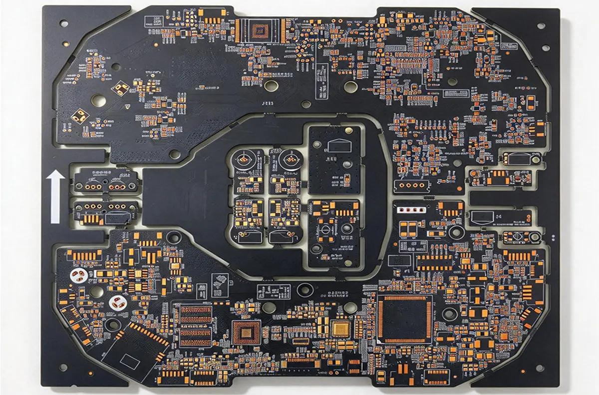
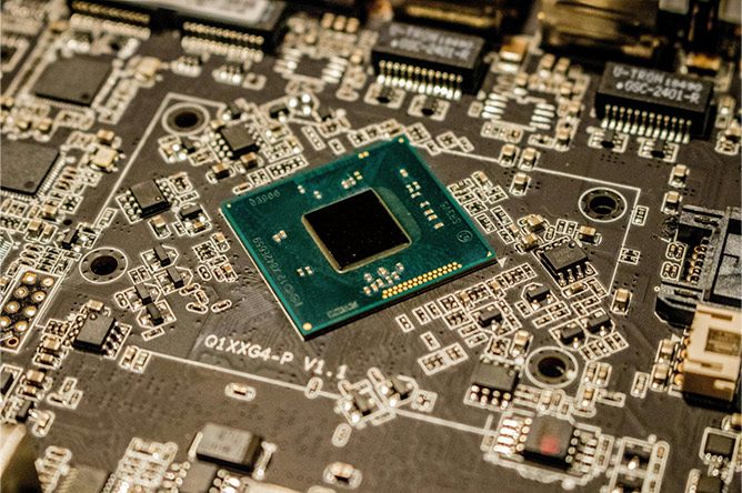
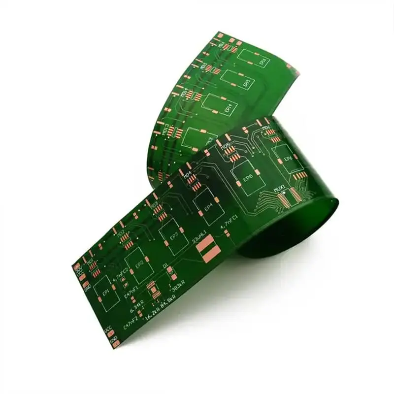
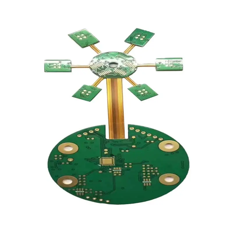
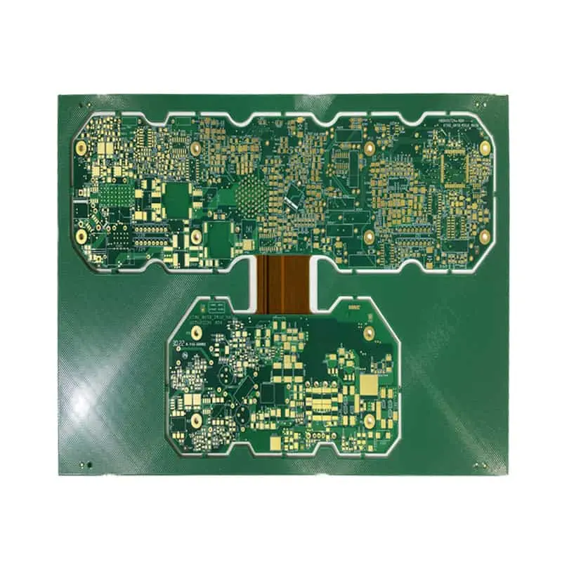
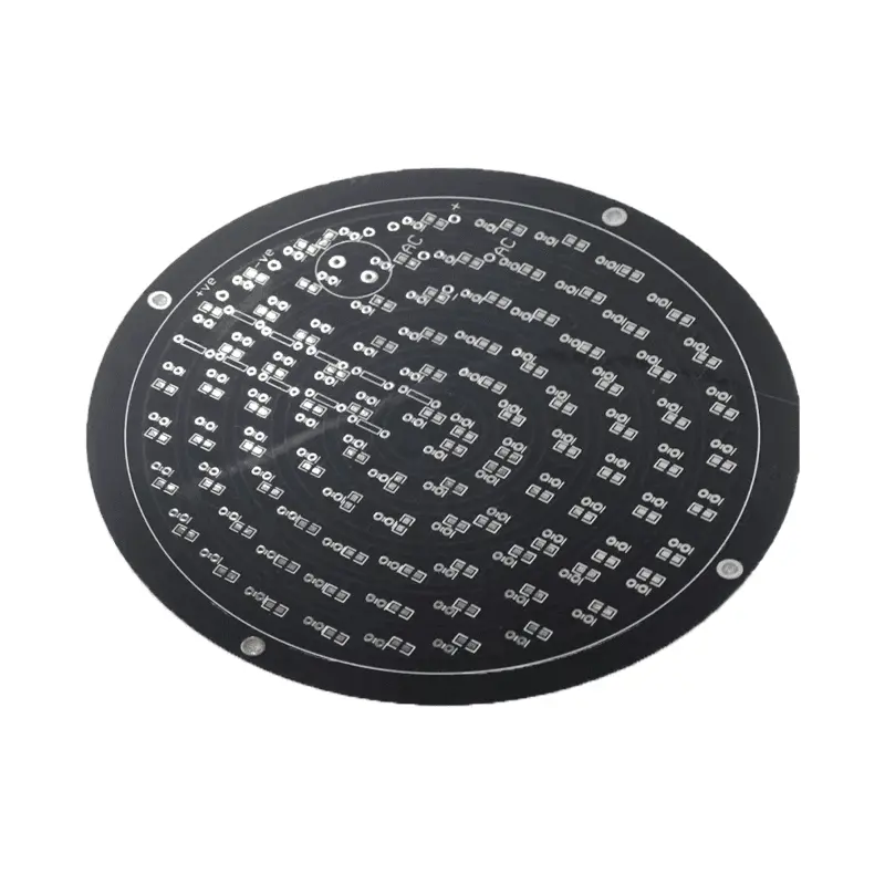
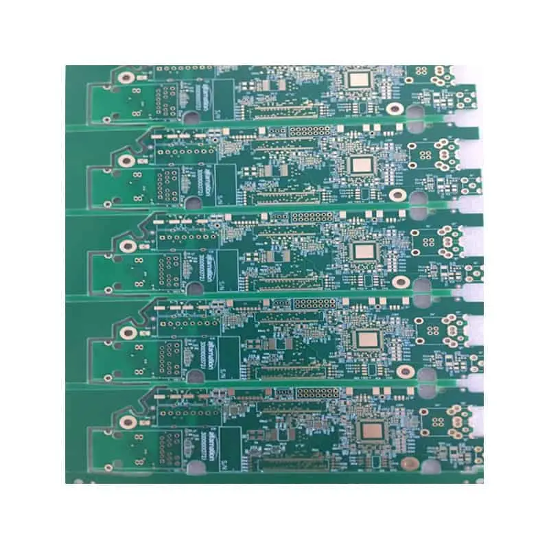
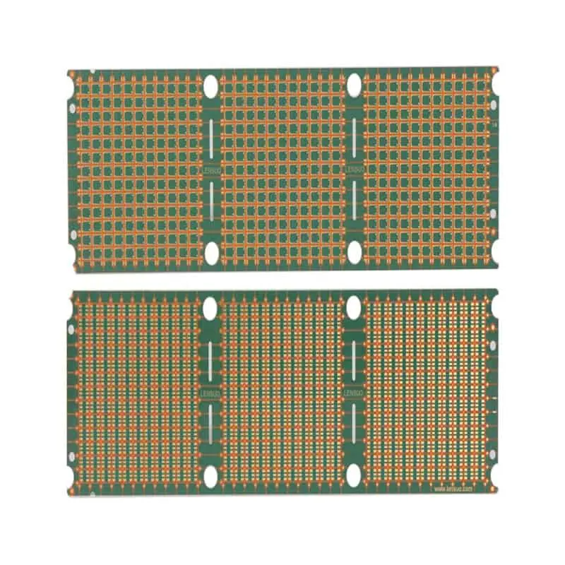
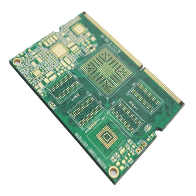
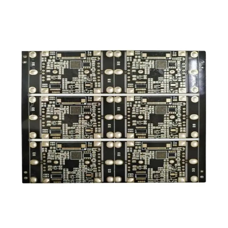
Selecting the optimal printed circuit board (PCB) architecture is a crucial technical and economic decision in electronics manufacturing. While single-sided boards offer lower upfront costs and multilayer boards provide ultra-high density, double-sided PCBs (two-layer PCBs) represent the ideal balance between circuit density, electrical performance, and cost-efficiency.
This guide provides engineering teams, procurement specialists, and hardware sourcing professionals with an in-depth breakdown of double-sided PCB technology, fabrication tolerances, design rules, assembly methodologies, and Design for Manufacturability (DFM) best practices.
1. What Is a Double-Sided PCB? Basics and When to Use It
A double-sided PCB consists of a conductive layer of copper deposited on both top and bottom sides of an insulating substrate (typically FR-4). Electrical connections between the two layers are established using Plated Through-Holes (PTH)—copper-plated vias that transport signals and power seamlessly across the board.
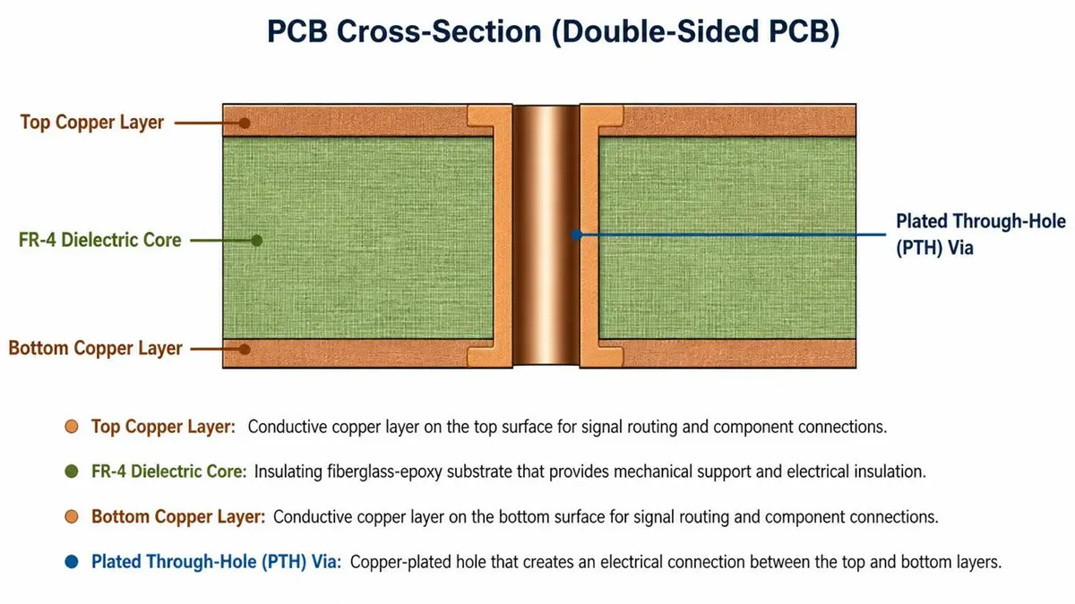
Double-Sided PCB Cross-Section Structure – Haoda Circuit
Single-Sided vs. Double-Sided vs. Multilayer Comparison
| Selection Metric | Single-Sided PCB | Double-Sided PCB | Multilayer PCB (4+ Layers) |
| Circuit Density | Low | Moderate to High | High to Very High |
| Cost Scale | Lowest | Cost-Effective Balance | High Premium |
| Assembly Complexity | Simple (SMT/THT) | Moderate (Dual-Sided SMT) | Complex |
| Signal Integrity | Poor | Good (Ground Fill/Shielding) | Excellent (Dedicated Planes) |
| Lead Time | Standard (1–3 days) | Fast Turn (24–48 Hours) | Standard (5–10 days) |
Engineering Sourcing Criteria: When to Choose Two-Layer PCBs
Upgrading from a single-sided PCB to a double-sided design allows engineers to cross trace paths without jumper wires, achieve proper ground plane shielding, and support surface-mount technology (SMT) on both sides.
Before jumping to a 4-layer or 6-layer board, consider a 2-layer design when:
Cost Efficiency vs. Density: The circuit requires routing density beyond a single layer, but component pin counts do not mandate high-density interconnect (HDI) or buried/blind vias.
Power Distribution: You require localized ground pours and wider power tracks on the bottom layer while running signal traces on the top layer.
Target Applications: Ideal for industrial controls, LED power supplies, automotive relay controllers, power meters, smart home IoT devices, and commercial telecommunications equipment.
US Onshore Sourcing Benefits: Fast-turn domestic quick-turn prototypes (24–48 hours) are drastically cheaper on 2-layer boards compared to multi-layer stacks, minimizing financial risk during NPI (New Product Introduction).
2. Double-Sided PCB Fabrication Process: Step-by-Step with Tolerances
Understanding the fabrication pipeline ensures realistic specifications during procurement and eliminates manufacturing delays.
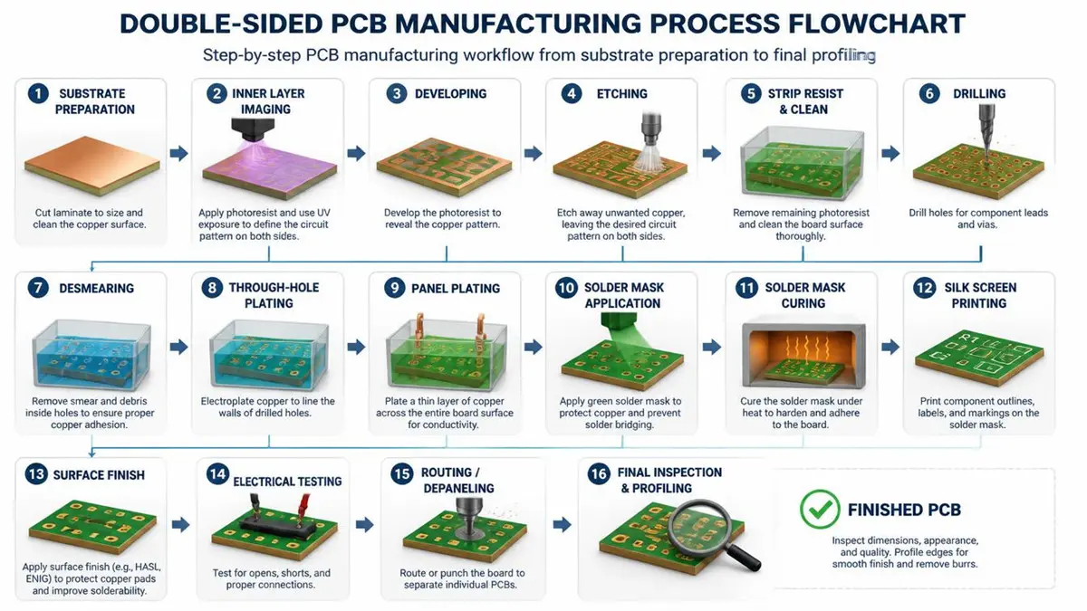
Step-by-Step Manufacturing Breakdown
Substrate Preparation: FR-4 laminate, pre-clad with copper foil (e.g., 0.5 oz, 1 oz, or 2 oz), is cut to panel size.
Drilling: High-speed CNC drills execute the via and hole pattern based on NC drill files.
Plated Through-Hole (PTH): A chemical electroless deposition of thin copper lines the drilled hole walls, followed by electroplating to establish electrical connectivity between top and bottom layers.
Patterning & Etching: Photoresist film is applied, exposed via UV light (or Direct Imaging), and non-circuit copper is etched away.
Solder Mask & Silkscreen: Liquid photoimageable (LPI) solder mask (green, black, white, blue) protects copper from oxidation and bridging, followed by silkscreen legend printing.
Surface Finish: Application of HASL, ENIG, or OSP protects exposed copper pads.
Profiling & Routing: V-scoring or tab routing separates individual boards from the panel.
Double-Sided PCB Manufacturing Process Flowchart – Haoda Circuit.
Fabrication Capabilities & Tolerance Matrix
| Specification Parameter | Standard Capability | Precision / Advanced Capability |
| Minimum Finished Drill Size | 0.20 mm (8 mil) | 0.15 mm (6 mil) |
| Minimum Line Width / Spacing | 4 mil / 4 mil (0.10 mm) | 3 mil / 3 mil (0.075 mm) |
| Min. Outer Annular Ring | 4 mil (0.10 mm) | 3 mil (0.075 mm) |
| Board Thickness Tolerance | ±10% (e.g., 1.6mm ±0.16mm) | ±8% |
| Copper Weight Options | 0.5 oz, 1.0 oz, 2.0 oz | 3.0 oz – 4.0 oz (Heavy Copper) |
| Hole Diameter Tolerance (PTH) | ±0.075 mm (±3 mil) | ±0.05 mm (±2 mil) |
| Hole-to-Edge Tolerance | ±0.20 mm (8 mil) | ±0.15 mm (6 mil) |
Gerber & CAM Export Checklist for Sourcing Engineers
To ensure zero-delay release to manufacturing, provide the following layers in your Gerber export (RS-274X or ODB++):
Top Copper (
.GTL) & Bottom Copper (.GBL)Top Solder Mask (
.GTS) & Bottom Solder Mask (.GBS)Top Silkscreen (
.GTO) & Bottom Silkscreen (.GBO)NC Drill File (
.DRL) with tool definitions and plated/non-plated identificationBoard Outline Layer (
.GKO/.GM1) specifying panelization or overall dimensions
3. Design and Layout Rules for Two-Layer Boards
Designing a high-performance double-sided PCB requires disciplined routing strategies to ensure signal integrity and power efficiency without adding extra manufacturing steps.
Trace Width & Current Carrying Capacity
Calculated using IPC-2221 standards, trace width must accommodate target temperature rises (ΔT). For 1 oz copper (35 µm) at a 10°C temperature rise:
1 Ampere: Minimum trace width ≈ 0.3 mm (12 mil)
3 Amperes: Minimum trace width ≈ 1.3 mm (50 mil)
5 Amperes: Minimum trace width ≈ 2.5 mm (100 mil)
Drill-to-Finished-Hole Compensation
During PTH manufacturing, electroplating deposits approximately 25 µm (1 mil) of copper onto the hole wall. To achieve a final finished hole size (PTH) of 0.3 mm, the drill bit size used is roughly 0.4 mm. Layout software usually handles this automatically, but maintaining proper annular ring pads prevents drill breakout during production.
Stackup Configuration & Impedance Control
While controlled impedance (e.g., 50 Ω single-ended, 100 Ω differential) is simpler on 4-layer boards with dedicated ground planes, it is achievable on 2-layer PCBs using microstrip or coplanar waveguide geometry over standard dielectric thickness.
Standard 1.6mm Two-Layer Stackup Example
Top Layer: Copper Foil (1 oz / 35 µm) — Signals & High-Current Lines
Dielectric Core: FR-4 Core (1.5 mm, Er ≈ 4.3–4.5)
Bottom Layer: Copper Foil (1 oz / 35 µm) — Continuous Ground Pour & Auxiliary Routing
Design Tip: To maintain controlled impedance on a 1.6mm 2-layer board, prefer Coplanar Waveguide with Ground (CPWG). Placing ground clearance rules close to the microstrip trace allows narrower, routable trace widths compared to wide standard microstrips.
4. Assembly, Testing, and Quality Control for Double-Sided PCBs
Populating components on both sides of a PCB demands deliberate assembly planning and quality check procedures.
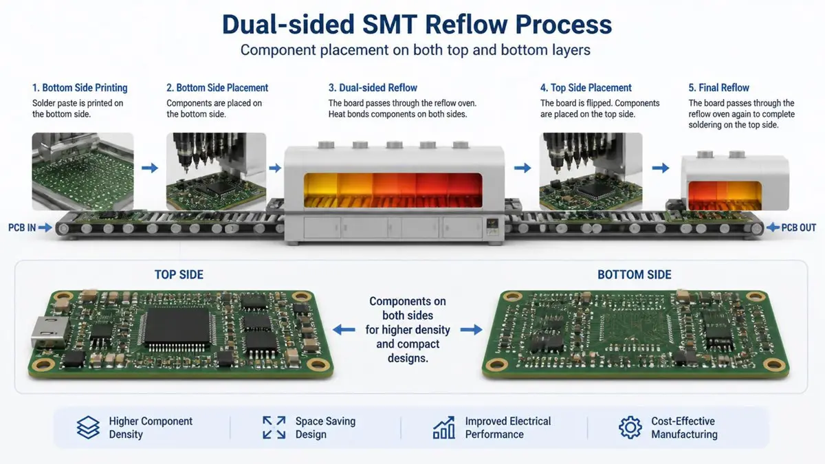
Double-Sided SMT Assembly Reflow Process – Haoda Circuit
SMT Reflow & Wave Soldering Strategies
When components exist on both sides:
Double Reflow Process: The side with lighter, smaller SMT components (typically passive 0603/0402 components, small ICs) is printed with solder paste, placed, and reflowed first. The board is flipped, and the primary/heavy side is processed. Surface tension of molten solder prevents bottom components from falling off during the second pass.
Heavy Bottom Components: Heavy inductors or large connectors on the bottom side require localized adhesive/glue application or customized dedicated assembly fixtures (pallets) to hold components during the second reflow pass.
Through-Hole Technology (THT): If through-hole parts exist on a dual-SMT board, selective soldering or wave soldering with custom masks is used to avoid disturbing pre-soldered SMT parts.
Inspection and Testing Coverage
Automated Optical Inspection (AOI): Checks both top and bottom layers for component placement accuracy, orientation, solder bridges, missing parts, and tombstoning. Achieves up to 95–98% visual error detection.
Flying Probe Testing (Prototyping): High-precision movable probes verify continuity, short circuits, and component values without expensive test fixtures. Ideal for low-volume and prototype batches.
In-Circuit Testing (ICT) (Mass Production): Bed-of-nails fixtures test electrical characteristics simultaneously across designated test points. Offers high coverage (98%+ electrical faults) and rapid testing cycles for volume manufacturing.
5. Cost, Lead Time, Thermal Management, and DFM Checklist
Cost Escalation & Lead Time Comparison
| Feature | 2-Layer Double-Sided | 4-Layer Multilayer | Upgrading Impact |
| Material Cost Factor | Baseline (1.0x) | 1.6x – 2.0x | +60% to 100% higher base material cost |
| Tooling & Setup Fee | Low | Moderate | Additional film/layer alignment |
| Standard Turn Time | 24 to 48 Hours | 3 to 5 Days | Shorter production cycle for 2-layer |
| Yield Rate | Extremely High (>99%) | High (>97%) | Lower risk of internal lamination defects |
Thermal Management Techniques on 2-Layer Boards
Without inner ground or thermal planes, thermal dispersion on 2-layer boards relies on top/bottom copper geometry:
Thermal Via Arrays: Place matrix thermal vias under hot IC pads (FETs, power regulators) connecting top and bottom copper pours.
Thicker Copper Options: Upgrade to 2 oz (70 µm) copper weight for high-current applications to lower conductor resistance and dissipation losses.
Surface Finish Selection:
ENIG (Electroless Nickel Immersion Gold): Ideal for fine-pitch SMT, BGA, and planar component mating.
HASL / Lead-Free HASL: Cost-effective, robust for standard SMT and hand-soldering.
OSP (Organic Solderability Preservative): Excellent flat surface at low cost, suitable for single-reflow or short shelf-life requirements.
DFM Checklist for Sourcing & Hardware Engineers
Before submitting files for fabrication, verify:
[ ] Minimum Clearance: Trace-to-trace, trace-to-pad, and pad-to-pad meet minimum manufacturer limits (≥ 4 mil).
[ ] Annular Ring Integrity: Pad size is at least 0.20 mm larger than the finished drill size to prevent drill breakout.
[ ] Silkscreen Clearance: No silkscreen ink overlaps onto SMT pads or PTH annular rings (> 2 mil clearance).
[ ] Copper-to-Board-Edge Distance: Keep copper at least 0.20 mm (8 mil) from the routed outline or V-cut score lines.
[ ] Panelization Alignment: Include tooling holes (3.2 mm non-plated), fiducial marks on panel borders, and V-score or tab-routing spacing.
Accelerate Your Production with Instant Quotes & Expert DFM Support
Ready to turn your double-sided PCB design into reliable, high-yield production units? Whether you need rapid prototype turnarounds or scaled volume manufacturing, our North American engineering and fabrication network delivers uncompromised quality, strict IPC Class 2/3 compliance, and transparent lead times.
Download Free Gerber/CAM Export Checklist & DFM Guide
Upload Your Files for an Instant Online Quote
Schedule a Free DFM Engineering Review with Our Specialists
Experience fast-turn 24-hour rapid prototyping and domestic manufacturing support. Request your quote today to validate drill sizes, impedance requirements, and assembly strategies before production.
Frequently Asked Questions (FAQ)
What are the key differences between double-sided PCBs, single-sided PCBs, and multilayer PCBs?
Double-sided PCBs feature conductive copper on two sides connected via plated through-holes (PTH). Single-sided PCBs have copper on only one side and cannot route intersecting traces without physical wire jumpers. Multilayer PCBs (4+ layers) contain internal signal/power ground planes separated by prepreg, offering higher signal density and superior EMI shielding at higher manufacturing costs.
How do I choose via types and drill sizes for a two-layer PCB to meet manufacturability and reliability?
For standard two-layer PCBs, use standard Plated Through-Hole (PTH) vias. Maintain a minimum drill diameter of 0.20 mm (8 mil) and an annular ring width of at least 0.10 mm (4 mil) to guarantee drill alignment accuracy and mechanical reliability across thermal expansion cycles.
What fabrication tolerances (drill, annular ring, board thickness, copper weight) should I specify when ordering double-sided PCBs in the U.S.?
Specify standard fabrication tolerances: drill diameter at ±0.075 mm (±3 mil), outer annular ring ≥ 4 mil, board thickness tolerance at ±10%, and standard copper weights of 1 oz (35 µm) or 2 oz (70 µm). Requesting non-standard tight tolerances unnecessarily increases scrap rates and procurement costs.
When components are placed on both sides, what assembly strategies (reflow, wave, fixtures) minimize soldering defects?
Use a double reflow process: populate and reflow the bottom side (with lighter, smaller SMT parts) first, then flip and process the top side. Surface tension holds lightweight parts in place. For heavy bottom-side components, use selective adhesive application or custom carrier fixtures/pallets.
Which inspection and testing methods (AOI, ICT, flying probe) are recommended for double-sided boards at prototype and production stages?
Use Automated Optical Inspection (AOI) on both top and bottom sides for all runs. For quick-turn prototypes and small batches, choose Flying Probe Testing due to zero NRE fixture costs. For high-volume mass production, switch to In-Circuit Testing (ICT) or functional test fixtures to achieve maximum test coverage and minimal per-unit test time.
How do cost and lead time for double-sided PCBs compare with upgrading to a multilayer board, and when is the upgrade justified?
Two-layer double-sided PCBs cost approximately 40% to 50% less in material and fabrication fees compared to 4-layer boards, with standard lead times as fast as 24–48 hours. An upgrade to a 4-layer board is justified only when tight EMI controls, controlled high-speed impedance matching, or extreme component density cannot be solved on 2 layers.
About Author
David Chen LinkedIn Profile
David Chen is a Senior RF/PCB Process Engineer at HAODA ELECTRONIC CO.,LIMITED with over 12 years of experience in high-frequency PCB fabrication, impedance-controlled stack-up design, and Rogers/PTFE laminate processing. He also boasts an extensive professional background in PCBA manufacturing, PCBA testing, and PCBA optimization, with specialized expertise in high-precision PCBA fault analysis and rigorous PCBA reliability testing. The author has worked with high-layer-count server PCB fabrication, ultra-low-loss backplane stackups, and thermo-mechanical reliability optimization for AI infrastructure projects involving 112G and 224G PAM4 architectures. Skilled in complex circuit design and cutting-edge advanced PCB manufacturing processes, he delivers solutions that elevate product durability and performance across industrial applications. His technical articles focusing on PCBA manufacturing workflows and testing methodologies are widely cited by industry peers and technical platforms, and have gained attention and recognition from industry colleagues.