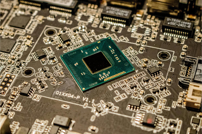
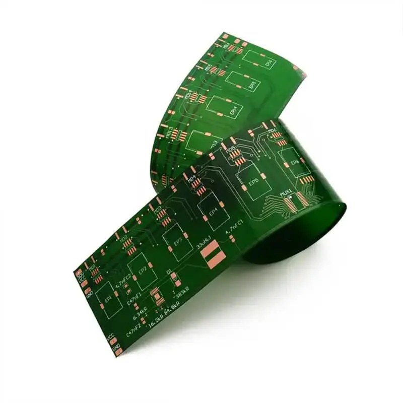
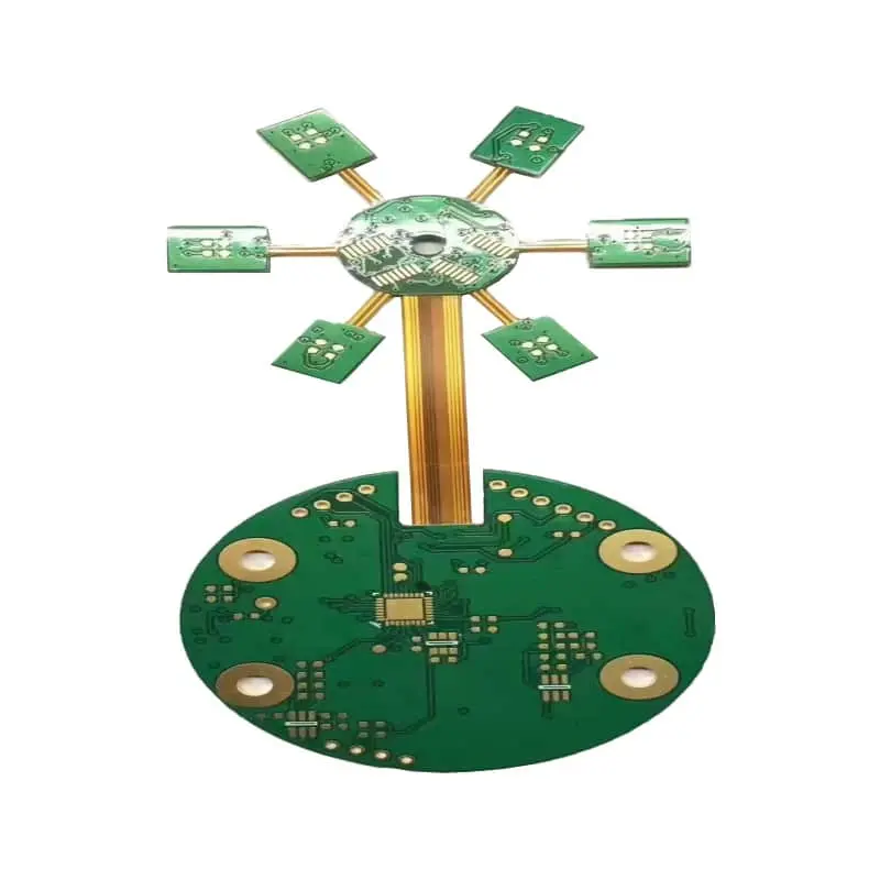
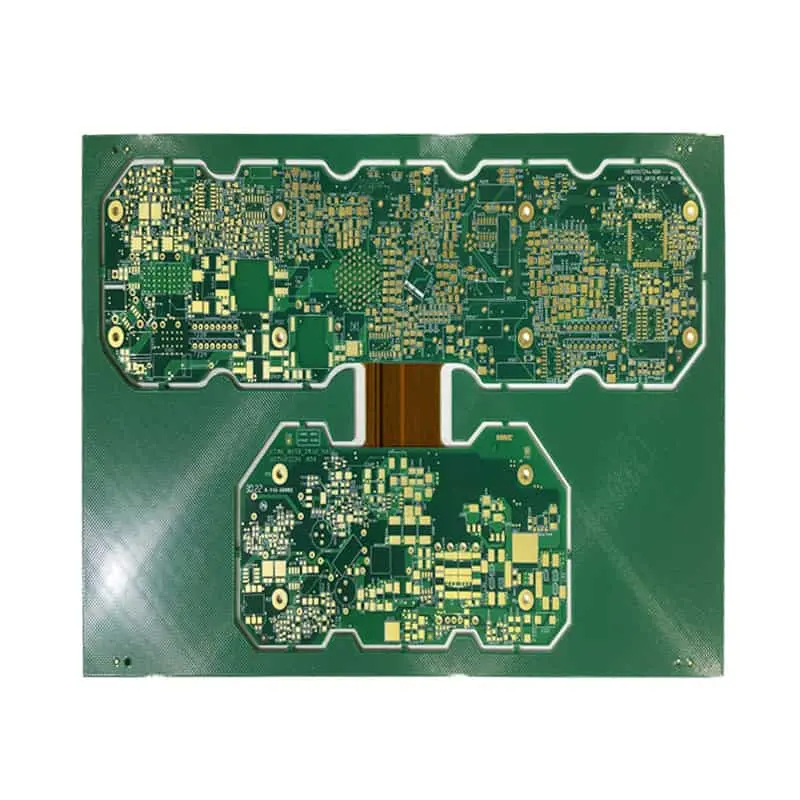
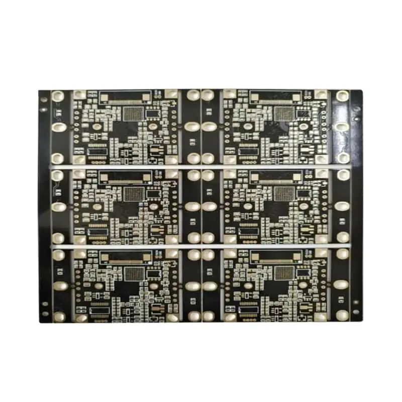
Low Volume PCB Fabrication requires balancing unit costs, initial setup overhead, turn time, and stringent quality control. Whether you are transitioning an engineering prototype to pilot production (10 to 500 units) or launching a specialized high-mix product, finding the optimal balance between speed and manufacturability is critical to project success. This comprehensive procurement guide provides a transparent roadmap covering cost structures, lead times, trade-offs, and essential Design-for-Manufacturing (DFM) best practices.

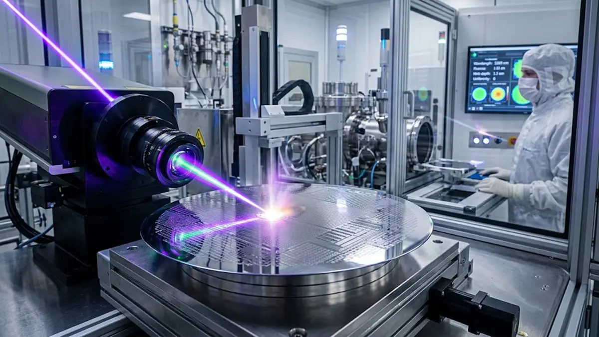
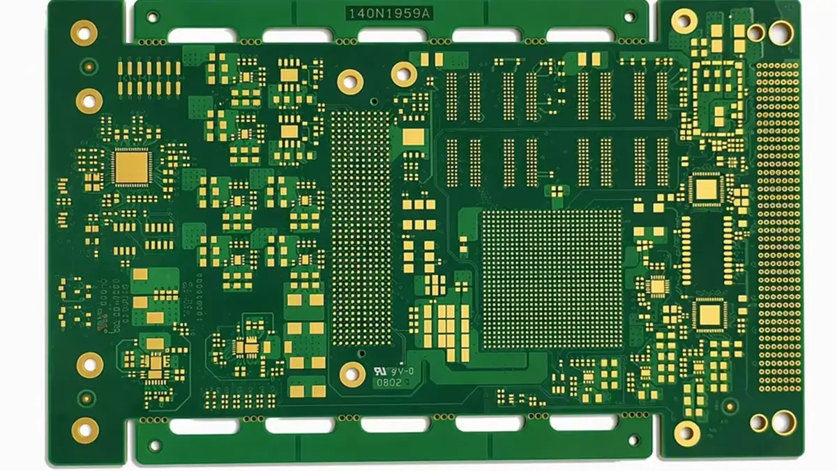
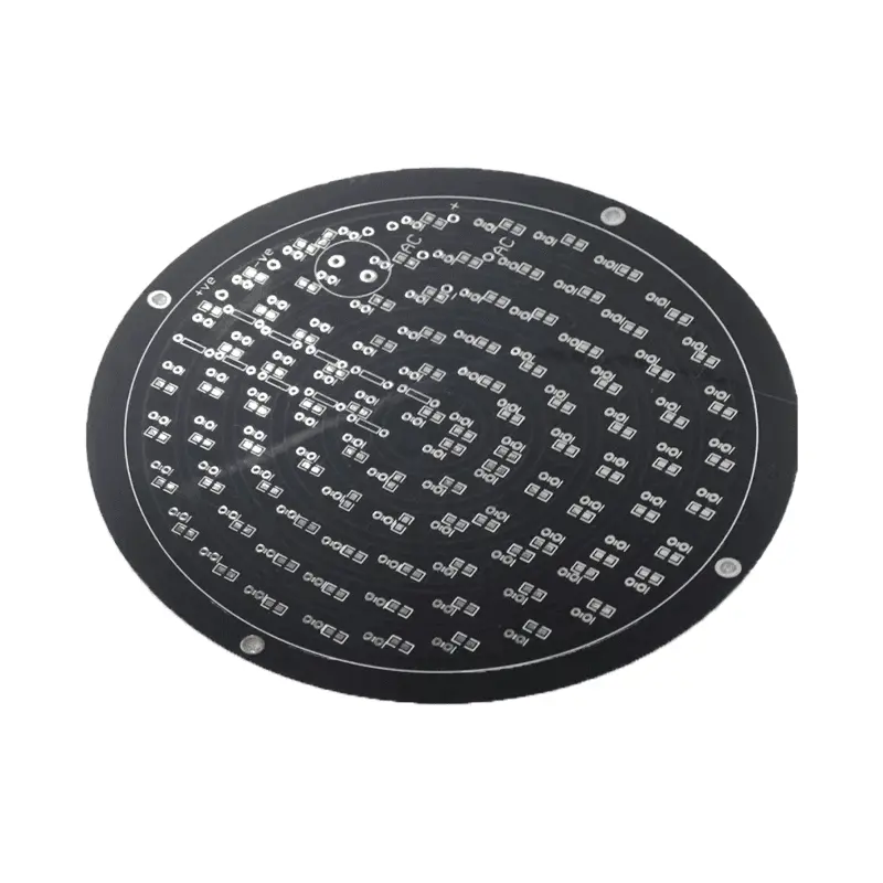
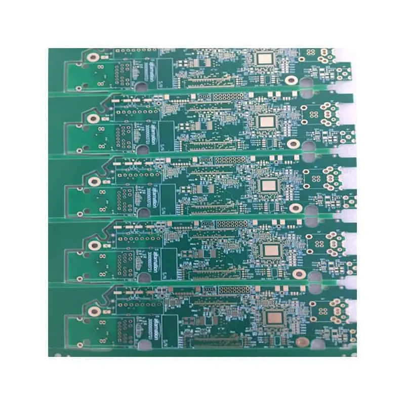
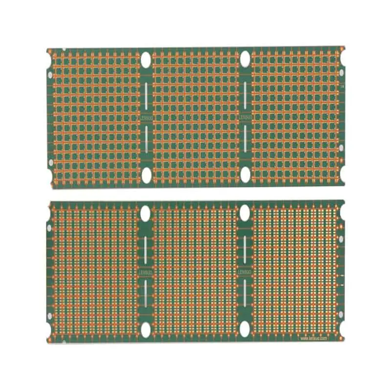
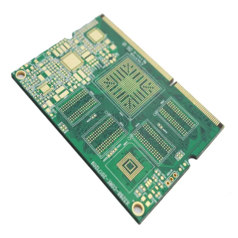
Low Volume PCB Fabrication & Quality Inspection at Haoda Circuit
Pricing & Cost Breakdown for Low-Volume PCBs
In low-volume manufacturing, non-recurring engineering (NRE) charges—such as tooling, stencils, photo-imaging setup, and programming—are distributed across a smaller quantity of boards. Understanding these driver variables allows engineering and procurement teams to optimize cost per unit effectively.
Key Cost Drivers
Layer Count & Stackup: Standard 2 to 4-layer FR-4 boards represent the base cost; jumping to 6+ layers or utilizing High-Density Interconnect (HDI) blind/buried vias significantly increases lamination and drilling steps.
Material & Copper Weight: Upgrading from standard FR-4 (Tg 150°C) to high-temperature FR-4 (Tg 170°C+), Rogers high-frequency laminates, or heavy copper (2 oz+) adds material premiums.
Surface Finish: Lead-Free HASL is the most economical, whereas ENIG (Electroless Nickel Immersion Gold), Hard Gold, or ENEPIG involve precious metal costs.
Panelization & Engineering Setup: Standard array sizes minimize edge waste. Custom routing or tight spacing increases scrap rate and tooling costs.
Cost Estimation Matrix by Production Scale
| Quantity / Scenario | Typical Volume | Estimated Bare Board Cost (4-Layer FR-4) | Estimated Assembly Cost (SMT + DIP) | Setup & Tooling Overhead (NRE) |
| Engineering Prototype | 1 – 5 pcs | $30 – $80 / board | $150 – $400 / batch | $50 – $150 (Waived on standard runs) |
| Short Run / Pilot | 10 – 50 pcs | $12 – $35 / board | $15 – $40 / board | $100 – $250 (Stencil + Setup) |
| Low-Volume Production | 100 – 500 pcs | $4 – $15 / board | $5 – $18 / board | Amortized across batch |
Cost Reduction Strategies for Short Runs
Shared Panelization: Combine multiple sub-boards onto a unified panel array to maximize material utilization.
Consignment vs. Turnkey Component Sourcing: Consign high-cost or specialized ICs while leveraging the fabricator’s standard active/passive stock.
Standardized Stackups: Select standard dielectric thicknesses and copper weights offered off-the-shelf by your vendor.
Onshore vs. Offshore Procurement: U.S. domestic fabrication eliminates international shipping delays and tariffs (e.g., Section 301 duties) for time-critical builds, whereas offshore sourcing yields lower unit prices on batches over 100 units.
Lead Times, Minimum Order Quantities, and Fast Turnarounds
Speed to market is often critical for low-volume production. Clear benchmarks help prevent unexpected delays caused by material procurement or component shortages.
Lead Time & MOQ Benchmarks
| Service Level | Bare PCB Lead Time | Assembled PCB Lead Time | Minimum Order Quantity (MOQ) |
| Quick-Turn Domestic (U.S.) | 24 – 72 Hours | 3 – 5 Business Days | 1 Piece |
| Standard Domestic | 5 – 7 Business Days | 7 – 10 Business Days | 1 Piece |
| Offshore Low-Volume | 7 – 10 Business Days | 10 – 15 Business Days | 10 – 50 Pieces |
Expedite Fees and MOQ Triggers
Expedite Drivers: Custom laminates (e.g., Rogers, Polyimide), heavy copper plating, sub-1-mil line spacing, or complex microvia drilling trigger additional expediting fees or standard lead time extensions.
MOQ Expectations: Bare boards rarely require MOQs beyond a single panel minimum, while turnkey assembly services may require minimum lot charges ($150–$300) to cover pick-and-place machine setup.
Practical Tips to Accelerate Delivery
Pre-order Long-Lead Components: Secure active ICs and microcontrollers prior to releasing Gerber files.
Standardize BOM Part Numbers: Use verified Manufacturer Part Numbers (MPNs) with active distributor availability (e.g., Digi-Key, Mouser, Arrow).
Parallel Panelization Approval: Approve array layout drawings simultaneously during initial DFM review.
Bare Board vs. Assembled: What to Order and When
Deciding between ordering bare printed circuit boards or complete turnkey surface-mount assembly (PCBA) depends on your team’s internal assembly capabilities, budget, and risk tolerance.
Project Requirement Decision Framework
Option A: Bare Board Fabrication Only
Best for teams with in-house SMT/soldering capabilities.
Recommended during early layout iterations or low component-count designs.
Offers the lowest initial setup fee.
Option B: Full Turnkey Assembly (PCBA)
Best for turnkey or consignment sourcing requiring complete SMT + THT assembly.
Recommended when high reliability is needed through factory-grade Flying Probe or ICT testing.
Minimizes internal labor and supply chain logistics management.
Trade-Off Analysis
| Factor | Bare Board Fabrication Only | Full PCBA (Assembly) |
| Initial Cost | Lowest initial setup fee. | Higher due to SMT stencils, feeder setup, and inspection. |
| Yield & Defect Risk | In-house soldering risks thermal stress, bridging, or ESD damage. | Factory-guaranteed yield with AOI and X-ray verification. |
| Supply Chain Burden | Buyer must source, kit, and verify all components manually. | Vendor handles procurement, attrition, and reel sizing. |
Component Sourcing Options
Consignment (Kitted): You supply all components to the factory. Best for proprietary ICs or pre-purchased inventory.
Partial Consignment: You provide critical/custom chips; the fabricator sources standard resistors, capacitors, and connectors.
Turnkey Procurement: The vendor manages full BOM procurement, leveraging bulk distribution pricing and guaranteeing component authenticity.
Essential File Checklist for Quoting & Production
To get an accurate, binding quote without delays, provide the following engineering package:
Fabrication Files: Gerber (RS-274X), ODB++, or IPC-2581 files.
Bill of Materials (BOM): Excel format including Quantity, Reference Designators, Description, Package, and exact Manufacturer Part Number (MPN).
Pick-and-Place (Centroid / XY Data): Component locations, layer side, and rotation angles.
Assembly Drawings & Test Specifications: Clear notes on silkscreen, thermal paste specifications, ICT fixture requirements, or functional testing steps.
Design-for-Manufacturing (DFM) Tips for Short Runs
Optimizing your layout for manufacturing reduces scrap rates and avoids costly re-spins during short-run fabrication.
Essential DFM Checklist
Trace Width & Clearance: Maintain a baseline of ≥ 5/5 mil (0.127 mm) for standard cost structures.
Minimum Annular Ring: Ensure a radius margin of ≥ 4 mil around vias.
Solder Mask Expansion: Maintain 2 to 3 mil clearance around SMT pads.
Silkscreen Clearance: Keep text at least ≥ 4 mil clear of pads to eliminate ink clipping.
Fiducial Placement: Include 3 non-symmetrical global fiducials per board/panel array.
Thermal Relief: Use 4-spoke layouts on power and ground planes for improved solderability.
Key Rules for Low-Volume Optimization
Trace Width & Clearance: Maintain a baseline of 5/5 mil for standard cost structures. Tightening to sub-3-mil increases photolithography scrap costs.
Vias and Annular Rings: Use a standard drill size of 0.3 mm (12 mil) or larger with an annular ring of at least 4 mil to ensure drill alignment margin.
Solder Mask & Silkscreen: Ensure solder mask dams between SMT pads are at least 4 mil wide to prevent solder bridging. Keep silkscreen text off exposed pads.
Fiducial Placement: Place 3 non-symmetrical global fiducial marks on panel corners and local fiducials for fine-pitch QFNs, BGAs, or 0201 passives.
Panelization with V-Score vs. Tab-Routing:
V-Scoring: Ideal for rectangular boards; reduces panel spacing and board unit costs.
Mouse Bites / Tab-Routing: Necessary for irregular geometries or delicate ceramic components to minimize mechanical stress during depaneling.
Quality Standards, Testing, and Compliance
Even on low-volume runs, adherence to recognized quality baselines guarantees reliability and compliance across industrial, medical, and aerospace applications.
Quality & Workmanship Baselines
IPC-A-600 Class 2 vs. Class 3: Class 2 is standard for commercial electronics; Class 3 imposes stricter plating thickness, annular ring drift, and voiding thresholds for high-reliability/mission-critical devices.
IPC-A-610 Class 2/3: Dictates criteria for component alignment, solder fillet shapes, and wetting standards during SMT/THT assembly.
Testing Methodologies
| Test Method | Setup Cost | Per-Unit Cost | Defect Coverage | Ideal Application |
| AOI (Automated Optical Inspection) | Low | Included | Visual defects, polarity, bridging | 100% of SMT assemblies |
| X-Ray Inspection (AXI) | Low | Low | BGA/QFN voiding, hidden solder joints | All leadless/BGA components |
| Flying Probe Testing | Zero | Moderate | Opens, shorts, resistance, capacitance | Prototypes & runs < 200 units |
| In-Circuit Testing (ICT) | High ($1k–$5k fixture) | Very Low | Comprehensive electrical & component value | Production runs > 500 units |
Case Study: Cost/Yield Trade-off
A medical device customer requested a 50-unit pilot run of a 6-layer HDI board containing two fine-pitch BGAs:
Scenario A (No X-ray / Flying Probe): Initial visual inspection showed 100% cosmetic pass, but functional testing revealed a 14% failure rate due to hidden BGA bridging. Field repair costs added $1,200 in labor.
Scenario B (Implemented AOI + AXI + Flying Probe): Adding $180 in total X-ray and probe testing identified 3 bridged BGAs on the line prior to encapsulation, achieving a 100% delivered yield and saving $1,000+ in rework.
Request a Fast & Accurate Low-Volume Quote
Ready to launch your next batch? Streamline your procurement process with our instant DFM analysis and multi-turn quote support.
Quote Package Submission Checklist
Gerber / ODB++ / IPC-2581 zip file
Complete BOM (.xlsx or .csv) with MPNs and quantities
Pick-and-Place (Centroid) coordinate file
Assembly & Testing specifications (if applicable)
Required target quantity (e.g., 10, 50, 100, 500 pcs) and lead time window
Get Started Today: Submit your manufacturing files for a Free Automated DFM & DFA Review with custom pricing within 24 hours.
Frequently Asked Questions (FAQ)
What typical price ranges should I expect per board for low-volume PCB runs in the U.S.?
For a standard 4-layer FR-4 board in quantities of 10 to 50 units, bare boards typically cost between $12 and $35 per unit in the U.S. Complete turnkey assembly adds approximately $15 to $40 per board depending on component density and fine-pitch ICs, plus small batch stencil and setup fees.
How do minimum order quantities (MOQs) differ between bare PCBs and assembled PCBs?
Bare PCB fabrication rarely carries a strict unit MOQ—you can order as few as 1 piece, though unit costs drop significantly at 10+ pieces. Assembled PCBs often incur a minimum setup/turnkey lot charge (typically $150 to $300) to cover SMT feeder loading and stencil production.
What are realistic lead time benchmarks for prototypes and small assembly runs?
Domestic U.S. quick-turn bare boards can be produced in 24 to 72 hours, with standard turns taking 5 to 7 business days. Assembled prototypes generally take 3 to 5 business days for quick-turn or 7 to 10 business days for standard turnkey service, provided component inventory is readily available.
When is flying-probe testing sufficient, and when do I need ICT for short runs?
Flying-probe testing requires no custom physical test fixture, making it ideal and cost-effective for short runs under 200–500 units. In-Circuit Testing (ICT) requires a bed-of-nails fixture costing thousands of dollars, which is only amortizable on volume runs over 500 to 1,000 units.
What key DFM rules reduce cost and improve yield for short-run PCB fabrication?
Maintaining trace width and spacing at or above 5/5 mil, using standard drill sizes (≥ 12 mil), avoiding buried/blind vias unless necessary, using standard 4-layer/6-layer material stackups, and providing proper fiducials on panel edges are the most effective ways to lower costs and maximize yield.
Should I choose a domestic U.S. supplier or an offshore vendor for low-volume work?
Choose a domestic U.S. supplier if you require rapid turnarounds (under 7 days), IP protection, ITAR/compliance controls, or zero tariff risk. Choose an offshore vendor for price sensitivity on quantities over 100 units where a 2 to 3-week lead time is acceptable.
What files and information should I include when requesting a quote to get accurate pricing?
You should include Gerber/ODB++ files, an Excel BOM with exact Manufacturer Part Numbers (MPNs), Pick-and-Place centroid files, an assembly drawing with special instructions, test requirements, and your target quantity and lead time requirements.
About Author
David Chen LinkedIn Profile
David Chen is a Senior RF/PCB Process Engineer at Shenzhen Hongda Circuit Technology Co., Ltd., with over 12 years of experience in high-frequency PCB fabrication, impedance-controlled stack-up design, and Rogers/PTFE laminate processing. He also boasts an extensive professional background in PCBA manufacturing, PCBA testing, and PCBA optimization, with specialized expertise in high-precision PCBA fault analysis and rigorous PCBA reliability testing. The author has worked with high-layer-count server PCB fabrication, ultra-low-loss backplane stackups, and thermo-mechanical reliability optimization for AI infrastructure projects involving 112G and 224G PAM4 architectures. Skilled in complex circuit design and cutting-edge advanced PCB manufacturing processes, he delivers solutions that elevate product durability and performance across industrial applications. His technical articles focusing on PCBA manufacturing workflows and testing methodologies are widely cited by industry peers and technical platforms, and have gained attention and recognition from industry colleagues.