PCB Layout & Routing Best Practices are the foundation of manufacturable, low-EMI printed circuit boards. Drawing on over 12 years of hands-on PCB manufacturing and design-for-manufacturing (DFM) engineering experience, this article outlines practical, production-proven workflows aligned with IPC industry standards. We break down component placement rules, trace routing discipline, copper pour techniques, DRC validation, and 2D/3D visual inspection. These guidelines help design engineers mitigate EMI, thermal hotspots, crosstalk and assembly defects, while enabling PCB buyers to submit cleaner Gerber packages, shorten lead times and stabilize production yield. All recommendations are validated by real prototype and mass production feedback from our PCB fabrication facility.
PCB Layout Principles Before Starting Component Placement

PCB Layout Principles Before Starting Component Placement
When applying PCB Layout & Routing Best Practices, your first step is to partition the circuit by functional blocks before placing components on the board canvas, following the proven “large first, small later; hard first, easy later” rule. Critical core circuits such as regulator ICs, high-power switches and sensitive analog circuits are placed first; passive components and interface connectors are arranged afterward.
Module Partitioning Logic: “Large First, Small Later; Hard First, Easy Later”
Proper block partitioning is the starting point of PCB Layout & Routing Best Practices. For switching regulators, the power loop forms the highest priority block. The input decoupling capacitor, freewheeling diode, inductor and output capacitor must stay tightly clustered around the regulator chip to minimize high di/dt switching loop area, which is the primary source of EMI noise in power boards.
Electrical Isolation Rules for Mixed-Signal & High-Voltage PCB
Separation of different signal domains is mandatory per IPC-2221 clearance requirements. Three common isolation strategies are widely used in production:
- High voltage and low voltage isolation with defined creepage and clearance;
- Analog signal domain isolated from digital switching circuits;
- High-frequency RF/timing traces separated from power loops.
Thermal hot components, high-frequency oscillators and power inductors require dedicated standalone zones to avoid coupling noise into low-level sensing signals.
Decoupling Capacitor Placement Rule
Power decoupling capacitors must be placed as close as possible to the power and ground pins of ICs, with ultra-short, direct traces. Long decoupling leads introduce parasitic inductance and degrade transient power response, a top defect found during our incoming DFM audit for power supply PCBs.
Professional PCB Routing Guidelines & Trace Discipline
Trace routing discipline is a core segment of PCB Layout & Routing Best Practices. When routing power and ground nets, follow the priority: ground traces > power traces > signal traces. Power and ground copper paths are widened according to IPC-2152 current-carrying capacity calculation to avoid overheating and voltage drop. Signal traces are kept narrow, short and direct.
Trace Width Priority: GND > Power Traces > Signal Traces
Ground traces carry the return current for nearly all signals, so they get the highest copper priority. Widen these paths early in your design to avoid thermal and voltage drop issues during mass production.
Critical Routing Rules to Reduce EMI & Antenna Effect
Several field-verified routing rules help you avoid common design mistakes:
- Keep trace length minimal and route traces aligned with pad exit direction;
- Eliminate floating stubs (floating dead-end traces) that create unintended antenna effects and radiate interference;
- Avoid 90-degree sharp corners; use 45° angles or arcs to reduce signal reflection and manufacturing acid trap risk;
- Follow the minimum loop principle: make the return path of every signal trace as compact as possible to suppress radiation and crosstalk.
Power Filter Routing Sequence for Buck Regulators
For buck regulators, the current flow sequence must be strictly controlled: the input current first flows through the decoupling capacitor for filtering, then enters the regulator IC. Do not insert long routing segments between the capacitor and the IC power pin. Feedback divider resistors for adjustable buck outputs must be placed near the FB pin, with feedback traces routed away from the switching node and inductor magnetic field.
Copper Pour & Polygon Fill Implementation for PCB
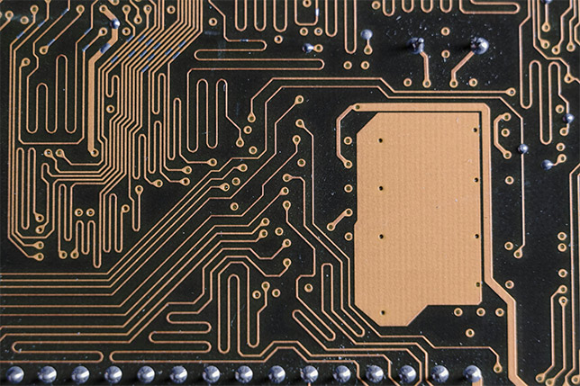
Copper pour is a key technique inside PCB Layout & Routing Best Practices to improve signal integrity and thermal performance. Copper pour (ground plane filling) is the standard practice for power and signal integrity. You can use polygon fill or solid pour to replace discrete traces for the same net. A continuous GND copper pour provides a low-impedance return path, improves heat dissipation and shields sensitive circuits from external noise.
When setting up copper pour rules in EDA software, configure clearance, thermal relief and connected net before pouring, to prevent short circuits and poor solderability.
EDA Design Rule Setup for Copper Pour and Clearance
Before routing and pouring copper, configure your PCB design rules inside EDA tools: safety clearance, trace width, annular ring, copper-to-pad clearance, silk screen spacing. These rule sets are the baseline for the subsequent automated DRC check and must match your PCB manufacturer’s process capability.
DRC Check, 2D & 3D PCB Preview for Pre-Fabrication Validation
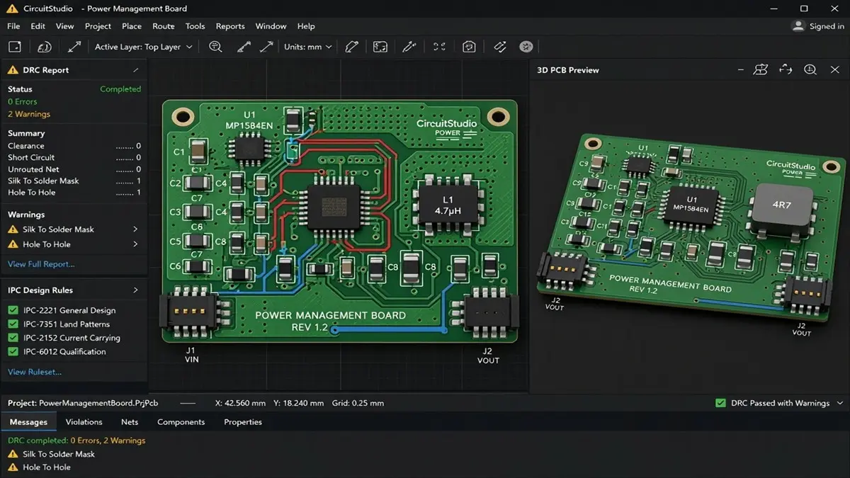
DRC Check, 2D & 3D PCB Preview for Pre-Fabrication Validation
No set of PCB Layout & Routing Best Practices is complete without final pre-production validation. Design Rule Check (DRC) is the mandatory quality gate before releasing files to manufacturing. A full DRC scan verifies:
- Trace width and spacing violations against IPC rules and fab limits;
- Silk screen clarity, reference designator placement and component marking consistency;
- Footprint and pin connectivity, missing pads or open nets;
- Thermal layout, isolation gap and high-voltage clearance;
- Short circuit, copper stub, and annular ring defects.
We also add project metadata including part number, revision, logo and version information before exporting Gerber files for PCB production.
2D Preview for Layout and Silkscreen Inspection
2D preview lets engineers review the finished board layout, trace topology, copper pour boundary and silk screen text. It is used to catch overlapping silkscreen, reversed pin labels and misaligned connector markings before manufacturing.
3D Preview for Mechanical Collision & Assembly Review
3D visualization is critical for mechanical fit and assembly validation. Engineers can check component height conflicts, connector orientation, and the overall board outline. For procurement teams, 3D renders also help communicate assembly requirements to contract assemblers and reduce misunderstanding during RFQ review.
Advanced EDA Features for High-Demand PCB Designs
Modern professional EDA platforms support advanced functions beyond basic single-track routing: differential pair routing, length matching tuning, fanout routing and multi-branch bus routing. Split-screen synchronous view (schematic + PCB side by side) speeds up cross-checking between schematic netlist and physical layout.
Welding assistant tools inside EDA can export interactive HTML inspection documents, which help assembly technicians and procurement teams verify component placement remotely on mobile devices.
FAQ for PCB Engineers & PCB Buyers
What core goals do PCB Layout & Routing Best Practices achieve?
A: PCB Layout & Routing Best Practices reduce EMI, minimize crosstalk, avoid thermal hotspots, prevent assembly defects and ensure your design meets IPC standards for reliable PCB fabrication.
Why is DRC check required before sending Gerber files to a PCB manufacturer?
A: DRC automatically validates whether your design meets IPC standards and the factory’s process limits. It catches short circuits, insufficient trace spacing, thin copper, clearance violations and silk screen errors. Skipping DRC will trigger DFM rejection, delay quotation and increase prototype rework cost.
What is the difference between polygon fill and copper pour on PCB?
A: Copper pour usually refers to a full-area ground/power plane poured over the board outline. Polygon fill is a localized copper shape assigned to a specific net. Both are used for low impedance connection, shielding and thermal dissipation, with different clearance rules configurable in EDA.
What are the IPC standards for PCB trace width and clearance?
A: IPC-2221 defines minimum electrical clearance for different voltage levels; IPC-2152 provides the calculation method for trace width based on copper weight, current and allowable temperature rise. Your PCB supplier will adjust these values according to their fabrication process capability.
How can PCB buyers reduce quotation delay and production yield risk when submitting RFQ?
A: Deliver complete Gerber files, clear DRC-clean design, specify copper thickness, surface finish, material grade and testing requirements. Attach 3D preview screenshots and DFM notes for power supply PCBs. Avoid floating stubs, 90° traces and unclear silk screen marks, which are common causes for fab feedback loops.
Is ground copper pour always recommended for power supply PCBs?
A: Yes, a solid GND plane is strongly recommended, but you must avoid splitting the ground plane under the high-speed switching loop. Broken ground planes force a large signal return loop and worsen EMI noise, even with copper pour applied.
Final Takeaway
Reliable PCB performance starts with disciplined layout planning guided by PCB Layout & Routing Best Practices, not post-routing fixes. Following module partitioning, isolation rules, priority routing, copper pour discipline and mandatory DRC + 3D preview will align your design with IPC specifications and reduce costly manufacturing rework. For OEM procurement teams, a clean, DRC-validated design package accelerates RFQ turnaround and stabilizes quality across prototype and mass production orders.
About Author
David Chen LinkedIn Profile
David Chen is a Senior RF/PCB Process Engineer at Shenzhen Hongda Circuit Technology Co., Ltd., with over 12 years of experience in high-frequency PCB fabrication, impedance-controlled stack-up design, and Rogers/PTFE laminate processing. He also boasts an extensive professional background in PCBA manufacturing, PCBA testing, and PCBA optimization, with specialized expertise in high-precision PCBA fault analysis and rigorous PCBA reliability testing. The author has worked with high-layer-count server PCB fabrication, ultra-low-loss backplane stackups, and thermo-mechanical reliability optimization for AI infrastructure projects involving 112G and 224G PAM4 architectures. Skilled in complex circuit design and cutting-edge advanced PCB manufacturing processes, he delivers solutions that elevate product durability and performance across industrial applications. His technical articles focusing on PCBA manufacturing workflows and testing methodologies are widely cited by industry peers and technical platforms, and have gained attention and recognition from industry colleagues.