PCB Impedance Control Technology
Terminology Glossary
TDR: Time Domain Reflectometer | VNA: Vector Network Analyzer | Dk: Dielectric Constant | Df: Dissipation Factor | Tg: Glass Transition Temperature | ENIG: Electroless Nickel Immersion Gold | HASL: Hot Air Solder Leveling
1. Basic Theory of PCB Impedance
1.1 Definition and Classification
PCB impedance refers to the total resistance to alternating current in transmission lines, mainly divided into single-ended impedance and differential impedance. Single-ended impedance is used for single signal lines, while differential impedance is designed for differential signal pairs, which is widely used in high-speed and high-frequency circuits.
The core difference: differential impedance is determined by the coupling effect of two signal lines, and its value is approximately twice the single-ended impedance under the same process conditions.
1.2 Core Calculation Formula (IPC-2221 Standard)
Microstrip Line (Single-Ended):
Z0 = (87 / √(Dk + 1.41)) × ln(5.98H / (0.8W + T))
Where: Z0=Impedance Value, Dk=Dielectric Constant, H=Dielectric Thickness, W=Line Width, T=Copper Thickness
All calculations must comply with IPC-2221 industry standards, which specify design parameters, tolerance ranges and test conditions.
2. Key Parameters Affecting Impedance
- Dielectric Thickness (H): The most sensitive parameter; thickness deviation directly causes impedance drift
- Line Width/Line Distance (W/S): Etching error control is critical; tolerance ±0.02mm for high-precision boards
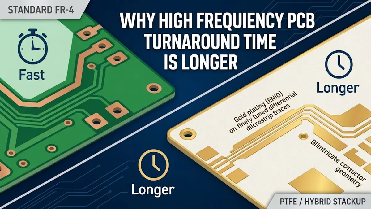
- Dielectric Constant (Dk): FR-4 Dk=4.2-4.8; high-frequency materials (PTFE/PPO) Dk=2.0-3.5
- Copper Roughness & Thickness (T): Low-profile copper foil reduces signal loss
- Environmental Factors: Temperature and humidity change Dk value, leading to impedance fluctuation
3. PCB Material Selection
| Material Type | Dk Value | Application Scenario | Core Advantages |
|---|---|---|---|
| FR-4 (Standard) | 4.2-4.8 | Consumer Electronics | Low cost, good processability |
| High-Tg FR-4 | 4.0-4.5 | Automotive/Industrial | High temperature resistance, low thermal expansion |
| PTFE | 2.0-2.5 | 5G/RF/Aerospace | Low loss, stable Dk |
Storage requirements: constant temperature (20±5℃), humidity <50%; baking parameters: 120℃, 4-6 hours to eliminate moisture absorption.
4. Stack-Up Design
Covers 2-layer, 4-layer, 6-layer and above high-layer PCBs, following symmetric design principles to avoid warpage and impedance deviation.
- 2-layer: Signal layer + Ground layer, suitable for low-speed circuits
- 4-layer: Top Signal – Ground – Power – Bottom Signal, standard for industrial control
- 6-layer+: Multi-ground layers for isolation, applied in 5G and high-speed servers
Mixed impedance design (single-ended + differential) requires independent parameter calculation and coupling effect control.
5. Core Manufacturing Process
5.1 Key Processes
- Etching: Control line width error within ±0.02mm
- Lamination: Precise thickness control, prevent layer deviation
- Drilling & Back-drilling: Reduce stub effect, avoid impedance resonance
- Solder Mask: Ink thickness and Dk affect impedance, cannot be ignored
- Surface Treatment: ENIG is preferred for high-speed boards; HASL for low-cost scenarios
5.2 Common Defects and Solutions
- Resin Smear: Optimize lamination pressure and temperature
- Layer Misalignment: Use optical alignment system
- Moisture Absorption: Strict baking before production
6. Impedance Testing and Quality Control
6.1 Test Equipment
- TDR: For rapid impedance value and fault location, mass production application
- VNA: For high-precision S-parameter test, laboratory and high-end products
6.2 Test Standards (IPC-6012)
- General products: impedance tolerance ±10%
- High-speed/automotive/medical: ±5% or ±3%
- Sampling: 100% full inspection for high-precision boards; 5-10% sampling for consumer boards
Calibration and shielding are required before testing to ensure data accuracy.
7. Typical Application Scenarios
- Automotive Electronics: Impedance tolerance ±3%, high-Tg materials, AEC-Q200 compliant
- 5G Communication: Low-loss materials, strict Dk control, differential impedance priority
- Medical Equipment: High reliability, full inspection, zero defect requirement
- Aerospace & Military: Extreme environment resistance, ultra-high precision control
8. Frequently Asked Questions (FAQ)
Q1: How to select impedance tolerance?
A: Determined by application: ±10% for consumer electronics, ±5% for industrial control, ±3% for automotive/5G/medical.
Q2: What is the impact of back-drilling on impedance?
A: Back-drilling removes signal stubs, reduces signal reflection, and stabilizes impedance performance.
Q3: Can ENIG completely replace HASL?
A: ENIG is better for high-speed circuits; HASL is still cost-effective for low-frequency and low-cost products.
9. Summary
PCB impedance control is a systematic project involving material selection, stack-up design, precision manufacturing and full-process testing. Strict compliance with IPC standards and parameter control is the key to ensuring impedance stability. With the development of high-speed and high-frequency electronics, impedance control will become more precise and standardized.