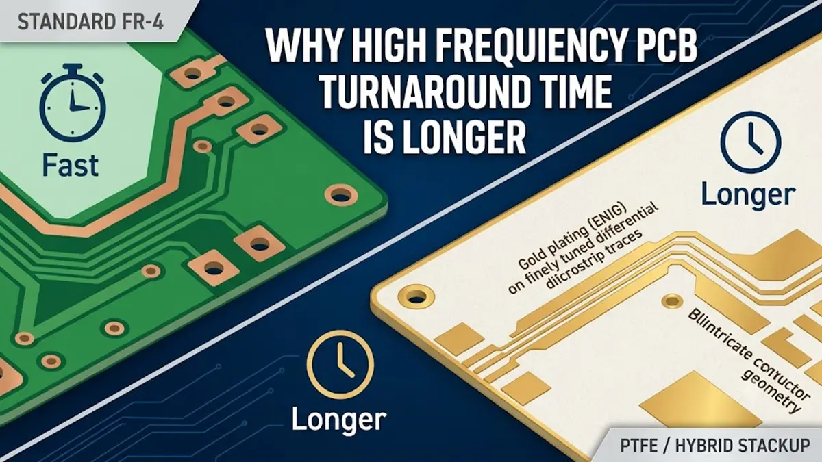
For standard prototypes, manufacturers can deliver high-frequency PCBs for 5G applications in 24 to 48 hours. For complex multi-layer or hybrid configurations, expedited delivery takes 3 to 5 days, while standard production runs typically require 2 to 3 weeks.
What Factors Determine the Turnaround Time for 5G High Frequency PCBs?
The turnaround time depends heavily on material availability, layer count, and structural complexity. When utilizing standard high-frequency laminates that are kept in stock, the standard lead times are structured as follows:
| PCB Configuration | Prototype (Expedited) | Standard Production |
|---|---|---|
| 2-Layer Rigids (Rogers/Teflon) | 24–48 Hours | 5–7 Working Days |
| Multi-layer High-Frequency (4–8 Layers) | 3–5 Working Days | 10–12 Working Days |
| Rigid-Flex / Hybrid (FR4 + Rogers) | 5–7 Working Days | 15–18 Working Days |
To hit these aggressive timelines, specific parameters must be locked in during the Design for Manufacturing (DFM) roadmap:
- Base Materials: Pre-stocked PTFE (Teflon) or Thermoset hydrocarbon laminates (e.g., Rogers RO4350B, RO3003, or Panasonic Megtron 6).
- Copper Weight: 0.5 oz or 1.0 oz to eliminate prolonged, non-standard electroplating cycles.
- Surface Finish: Electroless Nickel Immersion Gold (ENIG) or Immersion Silver (ImAg), avoiding time-consuming hard gold plating unless required for edge connectors.
What Are the Manufacturing Pain Points for 5G PCBs?
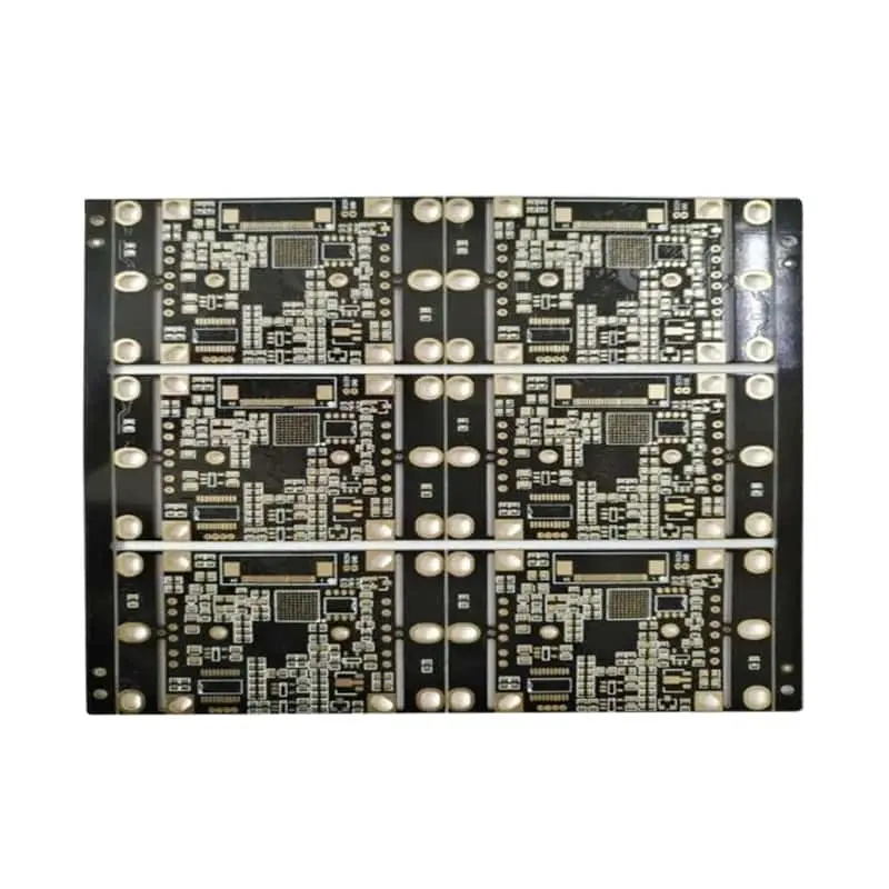
Manufacturing high-frequency PCBs for 5G applications introduces severe mechanical and chemical vulnerabilities that do not exist in conventional FR4 processing.
Material Dimensional Instability
Pure PTFE laminates (like Rogers RO3003) are incredibly soft and prone to “creeping” or stretching under mechanical stress. During panelization and baking, the material shifts. If a factory tries to rush the conveyor speeds through horizontal chemical lines, the tension can warp the core, resulting in misregistered inner layers.
Plasma Etching and Smear Removal
Due to the chemical inertness of PTFE, standard permanganate desmear lines cannot loosen the debris generated in drilled via holes. Manufacturers must use dedicated plasma desmear cycles (using a precise mix of Helium, Oxygen, and CF4 gas). If the plasma chamber cycle is rushed or poorly calibrated, resin smear remains, leading to intermittent open circuits or high-frequency signal degradation at the sub-6 GHz or mmWave thresholds (24 GHz – 40 GHz).
Micro-via Registration at High Density
5G architectures demand Blind and Buried vias alongside High-Density Interconnect (HDI) structures. Because high-frequency signals suffer from skin effect losses, any misalignment between the laser-drilled micro-via and the target pad will distort the characteristic impedance (50 Ω ± 5%), rendering the quick-turn batch entirely useless for RF telemetry.
In What Scenario Does 24-Hour Delivery Actually Apply?
Imagine a tier-1 telecom infrastructure engineer working on an emergency field patch for a 5G mmWave Small Cell G-NodeB base station operating at 28 GHz. The field test failed due to unexpected parasitic capacitance on the power amplifier output matching network.
The engineering team modifies the Gerber files at 8:00 PM, changing the trace geometry and opting for a 2-layer Rogers RO4350B substrate (0.020” core thickness) with a immersion silver finish.
By 11:00 PM, the CAM station validates the netlist. The factory isolates a pre-stocked sheet of RO4350B. Because this material is a ceramic-filled hydrocarbon (which processes similarly to rigid FR4), it bypasses the specialized plasma etching required for pure PTFE. It goes straight to direct laser imaging (LDI) for tracing, onto mechanical drilling, and immediately into an automated optical inspection (AOI) line. By 4:00 PM the next day, the boards are profiled via routing, vacuum packed, and placed on an overnight courier. Net fabrication time: 19 hours.
What Do Engineering Experts Say About Expediting 5G Layouts?
“When speed is paramount, don’t design custom stackups that force your fabricator to source exotic prepregs,” warns Senior RF Manufacturing Specialist, Dave Vance. “We see so many 5G prototypes delayed not because of fabrication complexity, but because the designer specified an obscure dielectric thickness that has a 6-week lead time from the material vendor.”
From our internal engineering playbook, hitting a 48-hour window on a hybrid multi-layer board (e.g., Rogers laminated to an FR4 sub-structure to save costs) requires strict compliance with the 3-to-1 rule:
- Keep the high-frequency material exclusively on the outer layers where the RF traces reside.
- Ensure that the mechanical drill aspect ratio does not exceed 8:1. Attempting a 10:1 or 12:1 aspect ratio on a fast turnaround forces the factory to slow down the drilling hit-rate to prevent drill bit deflection, instantly adding 12 hours of mechanical processing and inspection buffers to the floor schedule.
FAQ
Choosing Rogers RO3003 can extend expedited delivery times by 24 to 48 hours compared to RO4350B. RO3003 is a pure PTFE-based material that requires specialized plasma treatment for desmearing and a highly optimized drilling profile due to its soft, elastic nature. RO4350B is a thermoset hydrocarbon ceramic that behaves similarly to FR4, allowing factories to run it through standard fast-track chemical and mechanical lines without modifying parameters.
No. A 24-hour turnaround is virtually impossible for hybrid multi-layer PCBs. Hybrid stackups require multiple, distinct lamination cycles because FR4 and RF laminates press at different temperatures and pressures (185°C vs. over 210°C). The minimum expedited time for a high-quality hybrid multi-layer prototype is 3 to 5 days.
Yes. Standard PCB impedance tolerance is ±10%. If your 5G application demands a strict ±5% impedance tolerance, it requires the manufacturer to perform a mandatory first-article test run and make micro-adjustments to the etching line speeds. This engineering validation step adds at least 4 to 6 hours to the front-end CAM processing time.
Immersion Silver (ImAg) or Electroless Nickel Immersion Gold (ENIG) are the fastest finishes, easily fitting into a 24-to-48-hour window. ImAg is highly preferred for 5G because it lacks the magnetic nickel layer found in ENIG, which minimizes insertion losses at high millimeter-wave frequencies. Avoid Hot Air Solder Leveling (HASL) as it provides poor surface coplanarity for high-frequency components and ruins impedance consistency.
LDI eliminates the need for physical photo-tools (films), which saves 2 to 3 hours in setup time. More importantly, LDI dynamically scans the board and automatically adjusts the circuit pattern to match any slight material shifting or shrinkage that occurs in high-frequency laminates during baking. This ensures near-perfect registration on the first pass, preventing time-consuming scrap and re-runs.
About Author
David Chen https://www.linkedin.com/in/pcbcoming
David Chen boasts an extensive professional background in PCBA manufacturing, PCBA testing, and PCBA optimization, with specialized expertise in high-precision PCBA fault analysis and rigorous PCBA reliability testing. The author has worked with high-layer-count server PCB fabrication, ultra-low-loss backplane stackups, and thermo-mechanical reliability optimization for AI infrastructure projects involving 112G and 224G PAM4 architectures. Skilled in complex circuit design and cutting-edge advanced PCB manufacturing processes, he delivers solutions that elevate product durability and performance across industrial applications. His technical articles focusing on PCBA manufacturing workflows and testing methodologies are widely cited by industry peers, research institutions, and technical platforms, solidifying his reputation as a recognized technical authority in the global circuit board manufacturing sector.