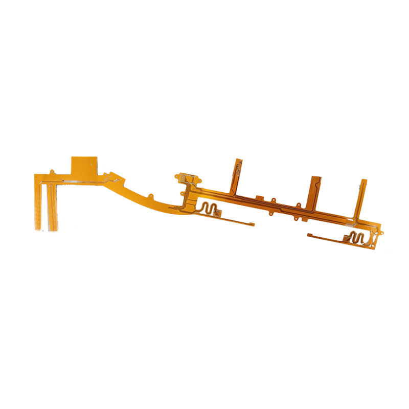
What Are the Key Differences Between Polyimide, LCP, PEEK and Specialty Flex PCB Substrates?
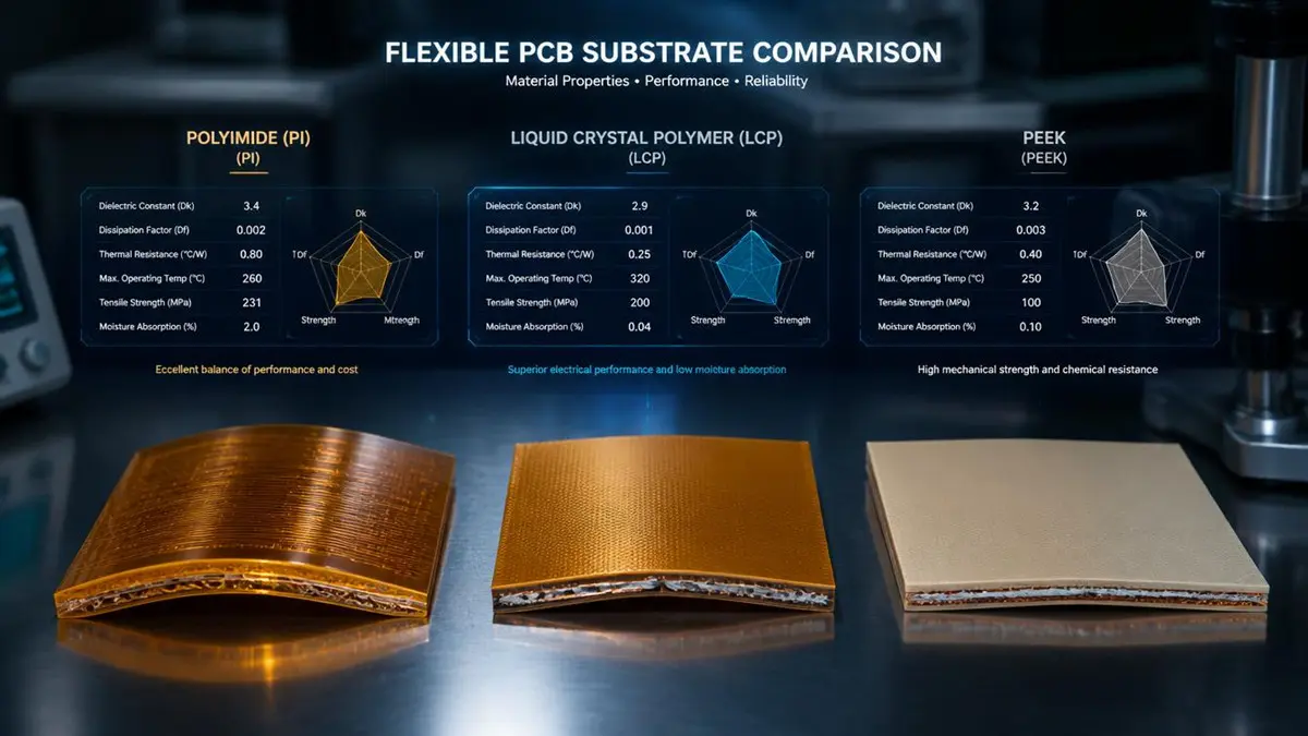
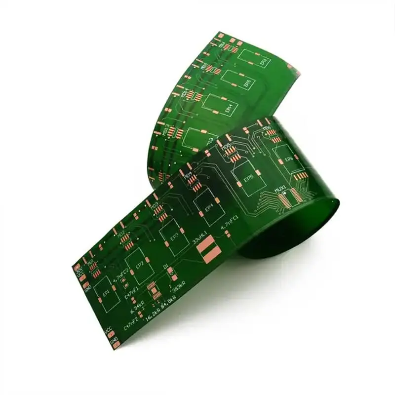
Flexible PCB Substrate Comparison: PI vs LCP vs PEEK
Polyimide is normally the best cost‑to‑reliability baseline; LCP is particularly strong for high‑frequency and moisture‑sensitive designs; PEEK is a premium option for high‑temperature, chemical‑resistant applications; and specialty low‑loss laminates are justified when RF or high‑speed insertion loss becomes a primary constraint.
| Material / Representative grade | Dk | Df | Tg / thermal characteristic | Tensile strength | Elongation | Thermal conductivity | Typical copper |
|---|---|---|---|---|---|---|---|
| Polyimide, Pyralux AP | ~3.2 @10 GHz | ~0.003 @10 GHz | Tg ~220°C | >345 MPa | >50% | Supplier‑specific | 18–70 µm common |
| LCP, Panasonic R‑F705S | 2.9 @19 GHz | 0.002 @19 GHz | Thermoplastic; high thermal stability | Grade‑specific | Grade‑specific | Grade‑specific | 12–18 µm example |
| PEEK film | ~3.1 @1 kHz* | ~0.004 @1 MHz* | Tg ~143°C; Tm ~343°C | 70–100 MPa** | Grade‑specific | ~0.29–0.32 W/m·K | Application‑dependent |
| HF‑grade / fluoropolymer‑class flex | ~2.1–3.0 typical* | ~0.0005–0.003 typical* | Grade‑dependent | Grade‑dependent | Grade‑dependent | Grade‑dependent | 9–35 µm common |
*Representative values vary substantially with formulation, frequency, reinforcement and test method. **Representative PEEK film range published by Goodfellow; not equivalent to a finished PEEK FCCL specification.
For a conventional automotive sensor harness or display interconnect, polyimide remains difficult to beat because it combines thermal stability, mechanical toughness, mature processing and broad supply availability. A representative Pyralux AP construction provides 3.2 Dk and 0.003 Df at 10 GHz, >345 MPa tensile strength and >50% elongation. Its published flexural endurance is at least 6,000 cycles under the specified test method.
LCP becomes more compelling when RF loss and moisture absorption matter. Panasonic’s FELIOS R‑F705S reports Dk 2.9 and Df 0.002 at 19 GHz, with 0.04% water absorption and an example using 18 µm ED copper. Panasonic specifically positions it for smartphone antennas, millimeter‑wave radar and high‑speed transmission.
PEEK occupies a different niche. Its melting temperature is approximately 343°C and its glass‑transition temperature is approximately 143°C for the referenced Victrex 90G grade, while Goodfellow lists PEEK film for flexible‑circuit substrates, aerospace insulation and medical applications.
From a procurement perspective, polyimide has the widest global supply base and normally the lowest material risk, followed by LCP specialty FCCLs and then application‑specific PEEK/HF constructions. Typical engineering sourcing windows should be treated as planning ranges rather than guaranteed lead times: roughly 1–3 weeks for stocked mainstream materials, 3–8 weeks for specialty FCCLs, and potentially 6–12+ weeks for custom or low‑volume high‑performance constructions.
For U.S. programs, do not treat “UL 94 V‑0” as equivalent to a complete PCB certification. UL 796/UL 796F construction recognition, the exact material system, copper thickness, assembly process and end‑product evaluation can all matter. UL’s database, for example, distinguishes flexible‑material constructions and identifies specific construction limitations.
Engineering recommendation: select the material only after defining the electrical frequency, minimum bend radius, required cycles, maximum process temperature, operating temperature and expected annual volume.
How Should Bend Radius and Cycle Life Be Used to Select a Flexible PCB Material?
Treat bend radius as a fatigue parameter, not simply a mechanical clearance dimension. A practical qualification should combine the neutral‑axis location, copper thickness, bend direction, bend angle, cycle frequency and environmental condition.
A useful first‑pass rule is:
| Application | Typical bend condition | Preliminary qualification target |
|---|---|---|
| Static bend / installation | ≥6–10 × finished flex thickness | 1–10 installation bends |
| Repeated equipment movement | ≥8–15 × flex thickness | 10,000–100,000 cycles |
| High‑cycle dynamic flex | ≥10–20 × thickness | 100,000–1,000,000+ cycles |
| Extreme thin‑flex dynamic design | Application‑specific | Validate experimentally |
These are engineering screening ranges, not guaranteed life predictions. Actual fatigue life can change by orders of magnitude when copper type, trace geometry, bend radius or temperature changes.
For example, a material may survive thousands of bends in a standardized test but fail much earlier in a product because the actual design concentrates strain at a via transition, solder joint or stiffener edge. That distinction is critical.
The copper is often the weak link. Rolled‑annealed (RA) copper generally provides better ductility for repeated flexing, while electrodeposited (ED) copper may be attractive for cost, availability and particular manufacturing requirements. Thin copper also reduces bending strain, but excessive reduction can create current‑density and manufacturability problems.
The IPC framework is particularly useful here. IPC‑6013 covers qualification and performance requirements for flexible and rigid‑flex printed boards, while IPC‑TM‑650 contains flexural‑fatigue and folding‑related test methods. IPC specifically identifies TM‑650 methods 2.4.3.1 and 2.4.3.2 for flexural fatigue of flexible wiring and flexible metal‑clad dielectrics.
For dynamic testing, define:
- Bend radius: actual product radius, not nominal CAD radius.
- Bend angle: for example, ±90° or ±180°.
- Frequency: typically selected to represent the product mechanism; 0.5–5 Hz is a practical laboratory screening range.
- Loading: pure bending versus bending plus tensile/compressive displacement.
- Environment: room temperature, elevated temperature, humidity or combined environmental exposure.
- Failure criterion: open circuit, resistance drift, visible copper cracking, insulation damage or delamination.
IPC’s newer bending‑durability test methodology also emphasizes reproducing the use‑case bending angle and radius and avoiding additional specimen tension during clamping.
Manufacturing pain point: A design team may specify “100,000 flex cycles” without specifying whether the test is performed before or after assembly. That is incomplete. Soldered components, stiffeners, coverlay transitions and connectors can radically change local strain.
A better procurement specification is:
“Minimum 100,000 cycles at R = 5 mm, ±90°, 1 Hz, after assembly, with continuity monitored continuously; no intermittent opens and resistance change ≤10%.”
That sentence is much more actionable than “high‑flex reliability required.”
How Do Dk, Df, Impedance, Tg and Thermal Conductivity Affect Flex PCB Performance?
Dk controls electromagnetic propagation and impedance; Df contributes to dielectric loss; dielectric thickness and copper geometry control characteristic impedance; Tg or high‑temperature behavior affects dimensional stability; and thermal conductivity controls how efficiently heat leaves localized hot spots.
For a simplified microstrip structure, impedance is strongly influenced by dielectric thickness, conductor width and effective dielectric constant. Consequently, a change in dielectric thickness of only several micrometers can become electrically significant on a thin flex circuit.
This is why “same nominal stackup” does not necessarily mean “same impedance.”
For a controlled‑impedance flex design, engineering should lock:
- Dielectric material and exact grade.
- Dielectric thickness after lamination.
- Copper thickness after processing.
- Trace width and etch compensation.
- Coverlay thickness.
- Copper roughness where high‑frequency loss matters.
- Target impedance and tolerance.
For high‑speed or RF flex circuits, LCP can offer a meaningful advantage. Panasonic reports Dk 2.9 and Df 0.002 at 19 GHz for R‑F705S and positions the material for millimeter‑wave radar and antenna applications. Its reported water absorption is only 0.04%, which helps reduce dielectric‑property drift in humid environments.
Polyimide is also capable of high‑frequency operation when a low‑loss grade and suitable copper are selected. DuPont’s Pyralux AP data shows approximately 3.2 Dk and 0.003 Df at 10 GHz, with high‑frequency insertion‑loss data published into the tens of GHz.
Scenario: Consider a wearable RF module operating around 24–30 GHz. A conventional adhesive‑based flex may introduce additional dielectric loss and dimensional variation. Moving to a low‑loss LCP construction can improve electrical stability, but the designer must then validate copper adhesion, laser processing, coverlay compatibility and connector assembly.
Thermally, the substrate is not normally a high‑conductivity heat spreader. A 0.29–0.32 W/m·K thermal conductivity reported for a referenced PEEK grade illustrates the limitation of polymer films compared with copper.
For a flex carrying high current, thermal design should therefore focus on copper cross‑section, copper area, thermal vias where rigid sections exist, component placement and heat transfer into the enclosure.
For soldering, qualification should reproduce the actual assembly thermal profile. IPC‑TM‑650 includes thermal‑stress and convection‑reflow simulation methods, while UL‑recognized flexible constructions can specify evaluated solder‑process temperatures and cycle counts.
A key engineering point is that Tg is not the same thing as maximum operating temperature. For thermoplastics such as LCP and PEEK, melting behavior, softening, creep and dimensional stability can be more useful design parameters than Tg alone.
How Do Manufacturing Constraints, FEA and Failure Analysis Determine the Best Flex PCB Material?
Material selection should be finalized together with the manufacturing process because adhesive cure, copper plating, coverlay lamination, soldering, handling and thermal expansion can create failures that cannot be solved by changing the circuit artwork alone.
1. Control the construction
An adhesive‑based flex normally has: Copper → adhesive → dielectric → adhesive → copper
An adhesiveless construction reduces the number of interfaces and can reduce overall thickness. A representative Pyralux AP construction uses an all‑polyimide adhesiveless dielectric and is offered with multiple dielectric and copper thicknesses.
However, adhesiveless does not automatically mean lower risk. The manufacturer still has to control lamination temperature, pressure, dimensional movement, copper adhesion and handling.
2. Select coverlay according to the bending zone
Coverlay is generally preferred where repeated flexing is expected because it forms a flexible protective dielectric structure. Soldermask can offer finer registration and easier selective processing, but its mechanical behavior and adhesion system must be considered in dynamic‑bend regions.
A common manufacturing mistake is placing a soldermask/coverlay transition directly at the highest strain location.
3. Model the real structure with FEA
A practical FEA workflow is:
Step 1 — Build the actual stackup. Include copper, dielectric, adhesive, coverlay, stiffener and component masses.
Step 2 — Select material models. Use elastic‑plastic or multilinear copper behavior where appropriate; use temperature‑dependent viscoelastic or hyperelastic data for polymers when long‑term deformation matters.
Step 3 — Apply realistic boundary conditions. Use the actual bend radius, displacement, clamp locations and component constraints.
Step 4 — Refine the mesh. Refine around copper traces, via transitions, stiffener edges, connector interfaces and sharp geometry changes. Avoid using an unnecessarily coarse mesh in these strain‑concentration regions.
Step 5 — Add temperature dependence. For soldering and thermal cycling, use temperature‑dependent modulus and CTE where supplier data is available.
Step 6 — Calibrate against physical testing. Measure strain, resistance change, bend cycles and failure location. Adjust the model only against measured evidence rather than tuning it to produce a desired answer.
4. Use a structured failure‑analysis flow
When a flex PCB fails, the fastest route is not immediately changing the material. Start with: Failure symptom → electrical test → visual inspection → X‑ray/CT where appropriate → metallographic cross‑section → microscope/SEM examination → material/process review → root‑cause confirmation.
Typical failure signatures include:
- Copper cracks at inner bend surfaces.
- Plating cracks around PTH transitions.
- Delamination between copper and dielectric.
- Coverlay lifting.
- Adhesive squeeze‑out or resin starvation.
- Via barrel cracking.
- Solder‑joint fatigue near rigid‑flex transitions.
- Dimensional shift causing connector misalignment.
- Thermal‑cycle‑induced resistance drift.
Manufacturing pain point: Many failures attributed to “bad polyimide” are actually caused by stackup strain, excessive copper thickness, an incorrect bend radius, poor coverlay termination, insufficient copper ductility or uncontrolled lamination movement.
For qualification, the supplier package should include the exact material datasheet, lot identification, certificate of conformance, UL status where applicable, copper type/thickness, adhesive or bondply specification, process capability data and sample test results.
IPC‑6013 provides the relevant performance framework for flexible and rigid‑flex boards, while IPC‑2223 addresses flexible/rigid‑flex design. IPC also maintains specific test methods for flexural fatigue, low‑temperature flexibility, peel strength, thermal stress and moisture‑related evaluation.
How Can You Turn Flexible PCB Material Selection Into a Faster RFQ?
Give the PCB manufacturer the mechanical, electrical, thermal and commercial constraints together instead of requesting a generic “flex PCB quote.”
For a fast engineering review, prepare:
- Minimum bend radius: R = ___ mm
- Required cycles: ___ cycles
- Bend angle: ±___°
- Operating frequency: ___ GHz
- Target impedance: ___ Ω
- Maximum operating temperature: ___°C
- Reflow peak: ___°C
- Copper thickness: ___ µm
- Finished flex thickness: ___ mm
- Expected annual volume: ___ pcs
- Target unit cost: $___
- Required qualification standard: IPC‑6013 / customer specification / other
- Required UL status: UL 796/UL 796F if applicable
A technically capable flex PCB supplier should be able to return more than a price. Useful deliverables include a material‑selection recommendation, stackup proposal, controlled‑impedance assessment, DFM feedback, preliminary FEA setup and qualification test matrix.
For prototype work, a practical engineering workflow can be divided into an initial 3–5 working‑day design/material review followed by approximately 10–15 working days for a prototype qualification package, depending on material availability, tooling and test scope.
The most important procurement question is therefore not:
“What is your cheapest flexible PCB material?”
It is:
“Which material‑stackup‑copper system gives us the required electrical performance and verified mechanical life at our production volume?”
That question usually produces a much more meaningful supplier comparison.
Procurement FAQ
Technical parameters and evaluation standards for engineers searching for Flexible PCB suppliers
What are typical Dk, Df and Tg values for polyimide, LCP and PEEK flex PCB materials?
| Material Type | Grade / Reference | Dielectric Constant (Dk) | Dissipation Factor (Df) | Thermal Properties |
|---|---|---|---|---|
| Polyimide (PI) | Pyralux AP | ~3.2 (@ 10 GHz) | ~0.003 (@ 10 GHz) | High Tg (grade dependent) |
| LCP | Panasonic R-F705S | ~2.9 (@ 19 GHz) | ~0.002 (@ 19 GHz) | Excellent moisture/thermal stability |
| PEEK | Standard Reference | Grade dependent | Grade dependent | Tg ~143°C | Tm ~343°C |
How can I estimate flex PCB bend cycles from bend radius?
Bend radius should be used as an initial screening parameter rather than a guaranteed fatigue-life equation. Dynamic testing is required to validate mechanical longevity.
| Design/Mitigation Factors | Testing Parameters to Define | Standard Reference |
|---|---|---|
| • Larger bend radius • Thinner copper layers • Ductile Rolled Annealed (RA) copper | • Actual bend radius & angle • Bending frequency • Operating temperature • Specific failure criteria | IPC-TM-650 (Flexural-fatigue testing methods) |
When should I choose adhesiveless flex PCB construction instead of adhesive-based construction?
| Construction Type | Key Advantages | Target Applications |
|---|---|---|
| Adhesiveless | • Reduced overall stackup thickness • Superior high-temperature performance • Tighter dimensional control • Lower dielectric loss | High-density, high-frequency, extreme thermal, or space-constrained designs. |
| Adhesive-Based | • Lower material cost • Compatible with established manufacturing processes | Cost-sensitive applications with standard thermal/electrical requirements. |
Is coverlay better than soldermask for flexible PCB reliability?
| Protective Layer | Primary Strengths | Best Used For |
|---|---|---|
| Coverlay | Integrated dielectric structure, superior mechanical flex fatigue resistance. | Repeated dynamic bending environments. |
| Soldermask | Fine pattern definition capability, selective processing options. | Static/flex-to-install applications or high-density component areas. |
Which IPC standards and tests should I specify for flexible PCB qualification?
Qualification requires a tailored test matrix aligned with the product’s mechanical and environmental duty cycle.
| Standard Category | IPC Specification | Purpose / Scope |
|---|---|---|
| Qualification Standard | IPC-6013 | Qualification and Performance Specification for Flexible Printed Boards |
| Design Standard | IPC-2223 | Sectional Design Standard for Flexible Printed Boards |
| Test Methods | IPC-TM-650 | Covering flexural fatigue, peel strength, thermal stress, solderability, moisture, and low-temperature flexibility |
For U.S. procurement teams: ask the supplier to provide the exact material manufacturer, grade, construction, copper foil type, dielectric thickness, UL recognition information where applicable, lot traceability and test method used for every critical property. This prevents a common sourcing problem: comparing two “polyimide flex PCBs” that use materially different dielectric, copper and adhesive systems.
About Author
David Chen https://www.linkedin.com/in/pcbcoming
David Chen boasts an extensive professional background in PCBA manufacturing, PCBA testing, and PCBA optimization, with specialized expertise in high-precision PCBA fault analysis and rigorous PCBA reliability testing. The author has worked with high-layer-count server PCB fabrication, ultra-low-loss backplane stackups, and thermo-mechanical reliability optimization for AI infrastructure projects involving 112G and 224G PAM4 architectures. Skilled in complex circuit design and cutting-edge advanced PCB manufacturing processes, he delivers solutions that elevate product durability and performance across industrial applications. His technical articles focusing on PCBA manufacturing workflows and testing methodologies are widely cited by industry peers, research institutions, and technical platforms, solidifying his reputation as a recognized technical authority in the global circuit board manufacturing sector.