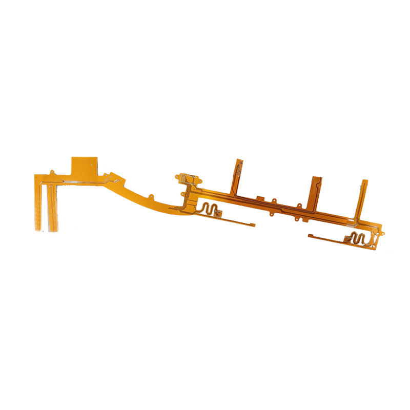
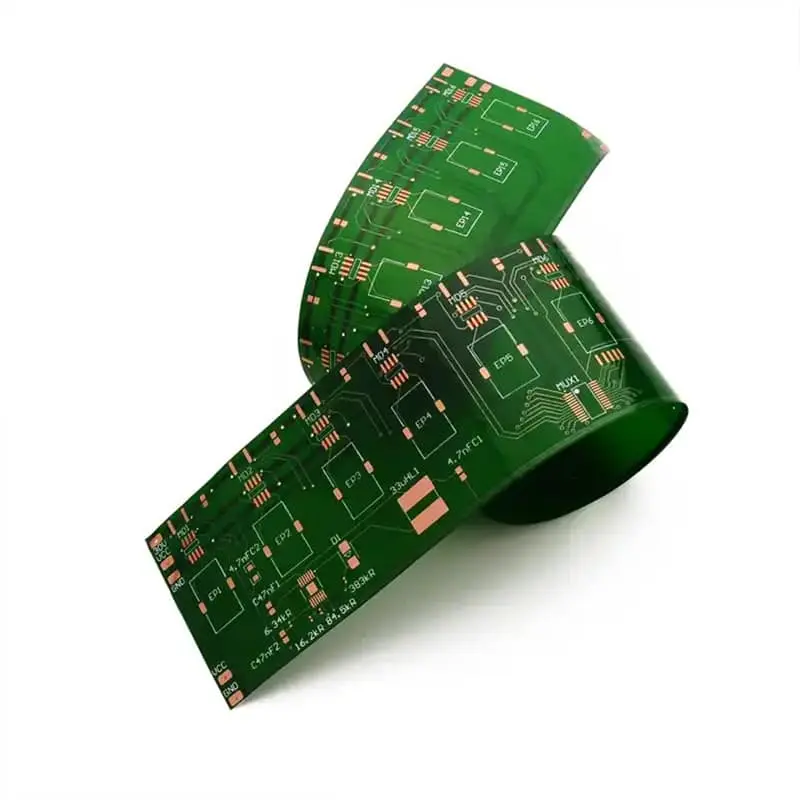
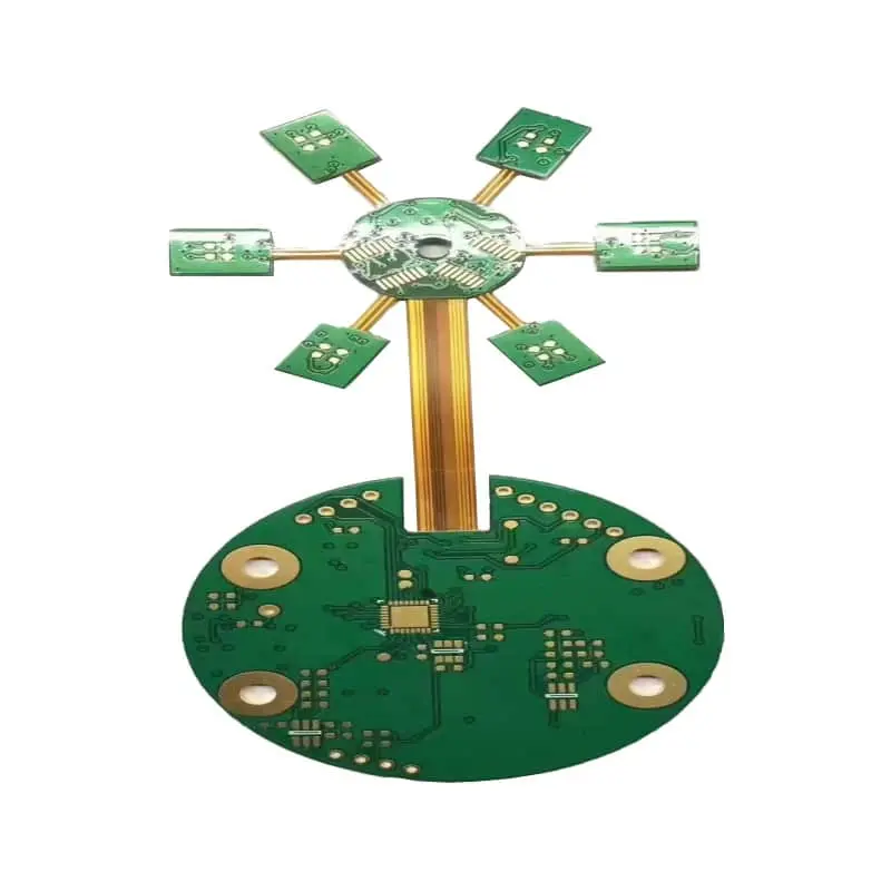
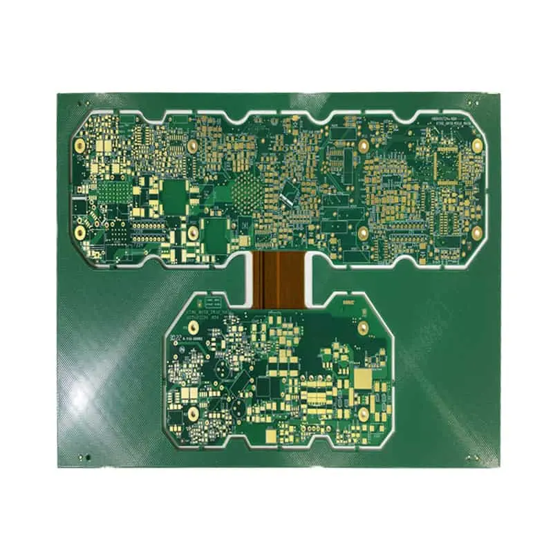
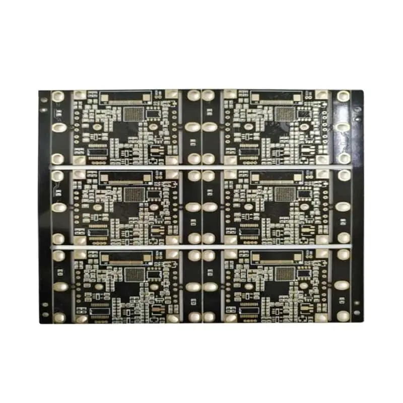
Flexible PCB Stacked Layer Structure Design for multilayer flexible PCB must balance electrical performance, bending reliability, manufacturability, thermal behavior, and cost. The correct stackup is therefore not simply a layer‑count decision—it is a coordinated mechanical, electrical, and manufacturing design.
What Are the Key Principles of a Multilayer Flexible PCB Stackup?
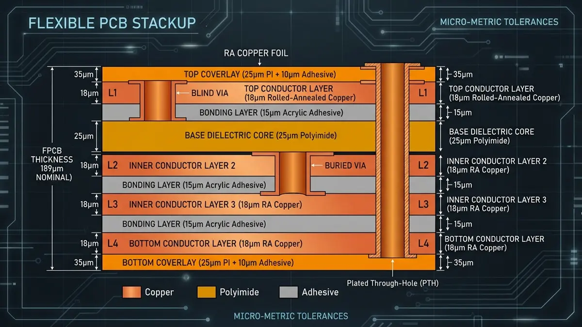
Detailed Cross-Section of a 4-Layer Flexible PCB Stackup
A reliable multilayer flex stackup should be designed in the order mechanical → electrical → manufacturing, with copper thickness, dielectric thickness, coverlay, bend zones, impedance requirements, and fabrication tolerances defined together.
Unlike a conventional rigid FR‑4 PCB, a flexible circuit must accommodate repeated deformation. Increasing layer count or copper thickness can improve routing and current capacity but normally increases total thickness and bending stiffness.
A practical 4‑layer flexible PCB can use the following starting structure:
| Layer | Material / Function | Typical Starting Thickness |
|---|---|---|
| Coverlay | Polyimide + adhesive | 25–50 µm |
| L1 | RA copper | 18 µm |
| Dielectric | Polyimide | 25–50 µm |
| L2 | RA copper | 18 µm |
| Core dielectric | Polyimide | 25–50 µm |
| L3 | RA copper | 18 µm |
| Dielectric | Polyimide | 25–50 µm |
| L4 | RA copper | 18 µm |
| Coverlay | Polyimide + adhesive | 25–50 µm |
For a rigid‑flex design, the flexible section may use a thin polyimide stack while the rigid section adds FR‑4 prepreg and stiff copper layers.
A 6‑layer rigid‑flex example could use 18 µm copper + 25–50 µm polyimide dielectric in the flex region, while the rigid region uses conventional multilayer dielectric materials.
The important point is to define the finished stackup, rather than simply specifying nominal material thicknesses. Lamination pressure, adhesive flow, copper distribution, and coverlay processing can change the final dielectric thickness.
For production designs, the stackup should be checked against applicable requirements of IPC‑6013 and IPC‑2223, together with the fabricator’s actual process capability.
A practical CAD decision sequence is: Mechanical envelope → bend zone → layer count → copper thickness → dielectric system → impedance → via structure → manufacturing tolerance → DFM review.
How Do You Control Impedance and Signal Integrity in a Stacked Flexible PCB?
Controlled impedance in multilayer flex depends primarily on trace width, copper thickness, dielectric thickness, dielectric constant, and the distance to the reference plane. Manufacturing variation in these parameters must be included in the impedance tolerance budget.
For a simple microstrip structure, an approximate impedance relationship can be expressed as:
Z₀ ≈ 87 / √(εᵣ+1.41) * ln( 5.98h / (0.8w+t) )
where:
- Z₀ = characteristic impedance
- εᵣ = effective dielectric constant
- h = dielectric thickness between trace and reference plane
- w = finished trace width
- t = copper thickness
Consider an illustrative 50 Ω microstrip:
- Copper thickness: 35 µm
- Dielectric thickness: 100 µm
- Dielectric constant: 3.5
- Trace width: approximately 0.165 mm
Using the simplified equation produces an impedance close to 50 Ω. This is a starting calculation, not a production guarantee. A field solver should be used for the final geometry because flexible materials, adhesive layers, copper roughness, soldermask/coverlay, and actual dielectric construction can alter the result.
Thickness tolerance is especially important. If a nominal 100 µm dielectric varies significantly during fabrication, the trace‑to‑plane distance changes and impedance shifts accordingly. Therefore, an impedance design table should include:
| Parameter | Nominal Example | Design Control |
|---|---|---|
| Target impedance | 50 Ω | ±10% or tighter if required |
| Copper | 35 µm | Control finished thickness |
| Dielectric | 100 µm | Specify finished thickness |
| Trace width | 0.165 mm | Account for etch compensation |
| Dk | 3.5 | Use supplier data at target frequency |
For high‑speed flex, verify the design with a 2D/3D electromagnetic field solver, followed by TDR or other controlled‑impedance verification during production.
Signal‑integrity debugging should check, in order:
- Actual dielectric thickness
- Finished trace width
- Copper thickness
- Reference‑plane continuity
- Via transition geometry
- Connector launch
- Bend‑zone deformation
- Material Dk and loss characteristics
How Should Bend Radius, Dynamic Flex, and Rigid‑to‑Flex Transitions Be Designed?
Bend radius should be selected from the finished flex thickness, copper thickness, layer count, and whether the application is static or dynamic. Dynamic applications require substantially more conservative mechanical design than one‑time folding.
A useful preliminary relationship is:
R ≥ t / (2ε)
where R is bend radius, t is total flexible‑section thickness, and ε is the allowable tensile strain.
For example, if a flex section is 0.20 mm thick and the allowable strain assumption is 0.5%, the theoretical radius is:
R ≥ 0.20 / (2 × 0.005)=20 mm
This illustrates why reducing flex thickness can dramatically improve bendability.
As an engineering starting point, designers can use a conservative bend‑radius matrix such as:
| Flex Construction | Static Bend Starting Point | Dynamic Bend Starting Point |
|---|---|---|
| 2‑layer, thin copper | ≥6× thickness | ≥10× thickness |
| 4‑layer | ≥8× thickness | ≥12–15× thickness |
| 6‑layer | ≥10× thickness | ≥15× thickness |
| Thicker/heavier copper | Increase radius | Increase substantially |
These are design starting ranges, not universal IPC limits. Actual requirements depend on copper type, grain structure, dielectric system, bend direction, temperature, and required cycle life.
For dynamic flex, the neutral mechanical axis should be considered. Copper traces positioned close to the neutral axis generally experience lower tensile and compressive strain.
At rigid‑to‑flex transitions, avoid placing vias, pads, sharp copper corners, or large component terminations directly in the high‑strain bend area. A controlled transition zone with appropriate adhesive, coverlay, stiffener, and routing geometry helps distribute mechanical stress.
During assembly, the flexible portion should be supported during SMT and reflow. Excessive unsupported movement, repeated thermal cycling, or bending while the assembly is hot can damage copper‑to‑polyimide interfaces.
How Do Manufacturing Tolerances and Via Choices Affect Multilayer Flex PCB Reliability?
Manufacturing variation directly changes electrical geometry and mechanical thickness, so the stackup should be designed around finished dimensions and process capability, not nominal CAD dimensions alone.
Typical variation sources include:
- Dielectric thickness variation
- Copper foil thickness variation
- Etching undercut or over‑etch
- Adhesive flow
- Layer‑to‑layer registration
- Coverlay registration
- Lamination thickness variation
- Via diameter and plating variation
For example, a reduction in dielectric thickness decreases the distance between a signal trace and its reference plane, potentially reducing impedance. Simultaneously, etching can reduce finished trace width and create another impedance shift.
A practical tolerance budget can therefore look like this:
| Parameter | Example Design Concern |
|---|---|
| Dielectric thickness | ±10–15% can materially affect impedance |
| Trace width | Etch variation changes impedance |
| Copper thickness | Changes both resistance and impedance |
| Layer registration | Critical around vias and fine‑pitch pads |
| Coverlay registration | Must maintain pad opening tolerance |
| Via diameter | Influences reliability and manufacturability |
Via selection should match both electrical and mechanical requirements. Through vias are generally simpler and economical but consume routing space. Blind vias can improve routing density but require additional process control. Buried vias are useful in rigid‑flex constructions where routing density justifies additional fabrication complexity. Laser microvias can provide high‑density interconnection in fine‑pitch designs, but drilling, desmear, copper plating, and reliability requirements become more demanding.
For flexible sections, designers should avoid assuming that a via structure proven in rigid FR‑4 will automatically provide the same reliability in a flex environment.
A recommended production verification flow includes: Stackup verification → material certificate review → dimensional inspection → AOI → X‑ray where appropriate → impedance testing → electrical test → microsection analysis for qualification → reliability testing.
The final acceptance criteria should reference the applicable IPC specification, customer requirements, and agreed fabrication capability.
How Should Thermal, Power, and EMC Requirements Be Managed in Multilayer Flex?
Power and ground layers should be designed around current, temperature rise, voltage drop, thermal spreading, and EMC simultaneously; simply increasing copper thickness is not always the best solution.
For a simplified resistive‑loss calculation:
P=I²R
and
R=ρ(L/A)
where I is current, R is conductor resistance, L is length, and A is copper cross‑sectional area.
For an illustrative 1 oz copper trace approximately 35 µm thick and 1 mm wide, the cross‑sectional area is about 0.035 mm². The resistance therefore depends strongly on trace length and copper temperature.
A preliminary current‑capacity comparison can be structured as:
| Copper Thickness | Trace Width | Relative Current Capability |
|---|---|---|
| 18 µm | 0.25 mm | Low |
| 18 µm | 0.50 mm | Moderate |
| 35 µm | 0.50 mm | Moderate |
| 35 µm | 1.00 mm | Higher |
| 70 µm | 1.00 mm | Higher still |
Actual allowable current must be calculated using the applicable temperature‑rise requirements and installation conditions. Flex circuits often have less thermal mass and less natural cooling than rigid boards, so thermal derating may be necessary.
For EMC, a multilayer flex can use dedicated ground structures, closely coupled signal/reference layers, shielding foil, controlled return paths, and appropriate chassis connections.
Avoid unnecessary gaps in reference planes around high‑speed signals. Where a signal changes layers, provide a low‑inductance return path whenever possible.
Surface finish is another engineering trade‑off. ENIG can provide a flat surface suitable for fine‑pitch assembly and exposed contact areas, while HASL can be economical but may be less attractive for fine‑pitch flexible applications. The choice should consider solderability, flatness, application environment, reliability, and cost.
Cost‑performance decisions should be made deliberately:
| Requirement | Typical Cost Driver | Design Strategy |
|---|---|---|
| More routing density | Layer count | Add layers only where necessary |
| Fine‑pitch interconnect | Microvias | Use only in high‑density zones |
| High‑speed signals | Low‑loss materials | Match material to data‑rate requirement |
| High current | Thick copper / wider traces | Balance current and flexibility |
| High EMI performance | Shielding / ground | Control return paths first |
| Tight mechanical envelope | Thin materials | Minimize total flex thickness |
How Can You Turn the Stackup Design Into a Production‑Ready PCB Specification?
Before requesting a quotation, provide the fabricator with the complete layer structure, material references, copper weights, finished thickness, impedance targets, bend requirements, via technology, and critical tolerances.
A production‑ready RFQ package should include:
- Layer‑by‑layer stackup
- Copper thickness for every layer
- Dielectric and coverlay thickness
- Material family and material number
- Finished board thickness
- Controlled‑impedance requirements
- Minimum trace/space
- Via technology
- Bend radius and bend‑cycle requirements
- Stiffener requirements
- Surface finish
- SMT/reflow requirements
- IPC acceptance class or customer specification
For engineering teams, a reusable multilayer flex stackup table, CAD template, impedance calculator, and mechanical/electrical/DFM checklist can significantly reduce design iterations.
When submitting an RFQ, attaching the stackup together with material numbers is especially useful because it allows the manufacturer to evaluate feasibility before pricing.
A typical prototype workflow is: Gerber/ODB++ + drill files → stackup review → DFM review → impedance review → quotation → prototype fabrication → electrical/mechanical inspection → validation → production release.
For complex rigid‑flex or high‑density multilayer flex designs, a dedicated DFM review before fabrication can identify stackup, bend‑zone, via, and tolerance problems before they become prototype failures.
FAQ
What minimum internal and external bend radii should I use for multilayer flexible PCBs?
As a preliminary starting point, static bends may use approximately 6–10× the finished flex thickness, while dynamic applications may require approximately 10–15× or more. The final radius should be established from copper thickness, layer count, material system, strain limits, and required cycle life.
How do I calculate controlled impedance for microstrip and embedded trace geometries?
Start with trace width, copper thickness, dielectric thickness, and dielectric constant, then use a transmission-line calculator or electromagnetic field solver. For production, validate the finished geometry through impedance testing such as TDR where applicable.
Which via types are suitable for rigid-flex and multilayer flex?
Through vias are generally the simplest option. Blind vias, buried vias, and laser microvias can increase routing density but introduce additional fabrication and reliability considerations. The appropriate choice depends on layer count, pitch, bend-zone location, and manufacturer capability.
How do dielectric thickness and copper etching affect impedance?
Both directly affect transmission-line geometry. Dielectric thickness changes the trace-to-reference-plane distance, while etching changes finished trace width. These variations should be included in the impedance tolerance budget rather than considered only after fabrication.
How can I estimate dynamic flex fatigue life?
Use the expected bend radius, total flex thickness, copper thickness, bend direction, temperature, and required cycle count as initial inputs. Prototype testing under the actual mechanical profile is strongly recommended because dynamic fatigue depends on the complete material and construction system.
How should I size power and ground structures in multilayer flex?
Calculate current capacity, resistance, voltage drop, and temperature rise, then evaluate thermal spreading and EMC return paths. Wider traces, additional copper layers, parallel conductors, or thicker copper can increase current capability, but these solutions must be balanced against flexibility and total thickness.
About Author
David Chen https://www.linkedin.com/in/pcbcoming
David Chen boasts an extensive professional background in PCBA manufacturing, PCBA testing, and PCBA optimization, with specialized expertise in high-precision PCBA fault analysis and rigorous PCBA reliability testing. The author has worked with high-layer-count server PCB fabrication, ultra-low-loss backplane stackups, and thermo-mechanical reliability optimization for AI infrastructure projects involving 112G and 224G PAM4 architectures. Skilled in complex circuit design and cutting-edge advanced PCB manufacturing processes, he delivers solutions that elevate product durability and performance across industrial applications. His technical articles focusing on PCBA manufacturing workflows and testing methodologies are widely cited by industry peers, research institutions, and technical platforms, solidifying his reputation as a recognized technical authority in the global circuit board manufacturing sector.