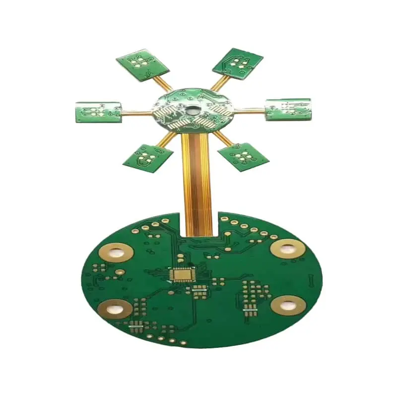
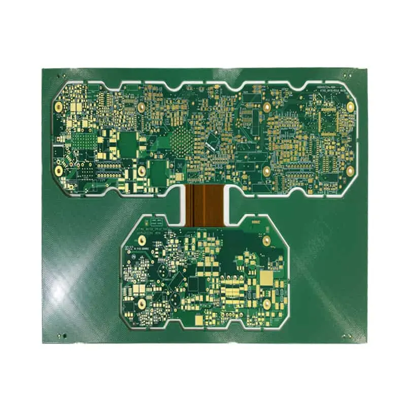
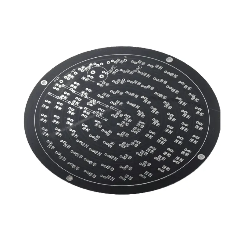
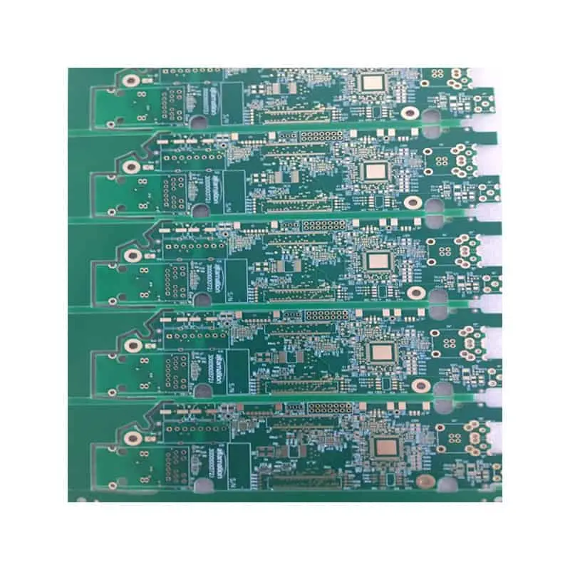
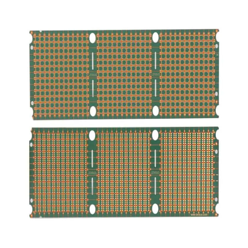
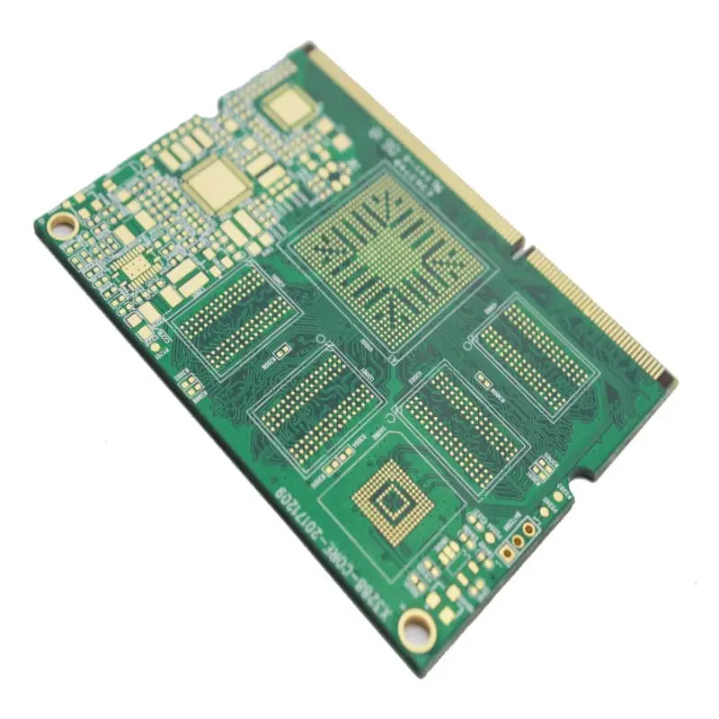
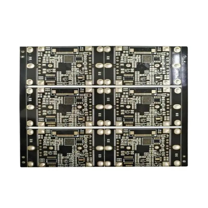
Carbon film PCBs combine the mechanical reliability of a conventional printed circuit board with the cost efficiency of printed carbon conductive ink. Whether you are sourcing membrane-switch contact pads, resistive traces, or sliding-contact elements for automotive, medical, or consumer products, this guide gives you the quantified specifications, process windows, and test requirements you need to evaluate suppliers and issue a purchase order with confidence.
What Is a Carbon Film PCB? Electrical Properties and Specs
A carbon film PCB is a standard rigid (FR-4), flexible (PI/PET), or metal-backed substrate on which conductive carbon ink is printed and cured to form pads, traces, or resistive elements. Unlike silver- or copper-based inks, carbon inks trade conductivity for cost, wear resistance, and contact reliability — which is exactly why they dominate keypad contacts, potentiometer tracks, and slider elements.
Key electrical parameters, with the measurement conditions stated explicitly:
Sheet resistance: 15–100 Ω/sq for standard graphite/carbon inks at a 10–25 µm dry film thickness; high-resistance formulations reach 500–1,000+ Ω/sq. By comparison, silver inks measure 0.005–0.05 Ω/sq at comparable thickness — roughly three orders of magnitude lower.
Volume resistivity: 0.005–0.1 Ω·cm, measured per ASTM D257 on a cured coupon of defined geometry.
Contact resistance: 10–100 mΩ against gold-plated or nickel-plated pads under 100–200 g contact force.
Temperature coefficient of resistance (TCR): −50 to −300 ppm/°C (negative). If you are designing a precision divider or potentiometer, this drift must be budgeted in your tolerance analysis.
Test references: sheet resistance per ASTM F390/F84 four-point-probe methods; qualification against IPC-6012 Class 2 or 3, as applicable.
Always require suppliers to state sheet resistance at a specified cured thickness — a number without a thickness is not comparable.
Deposition and Fabrication Methods: From Screen Printing to Laser Ablation
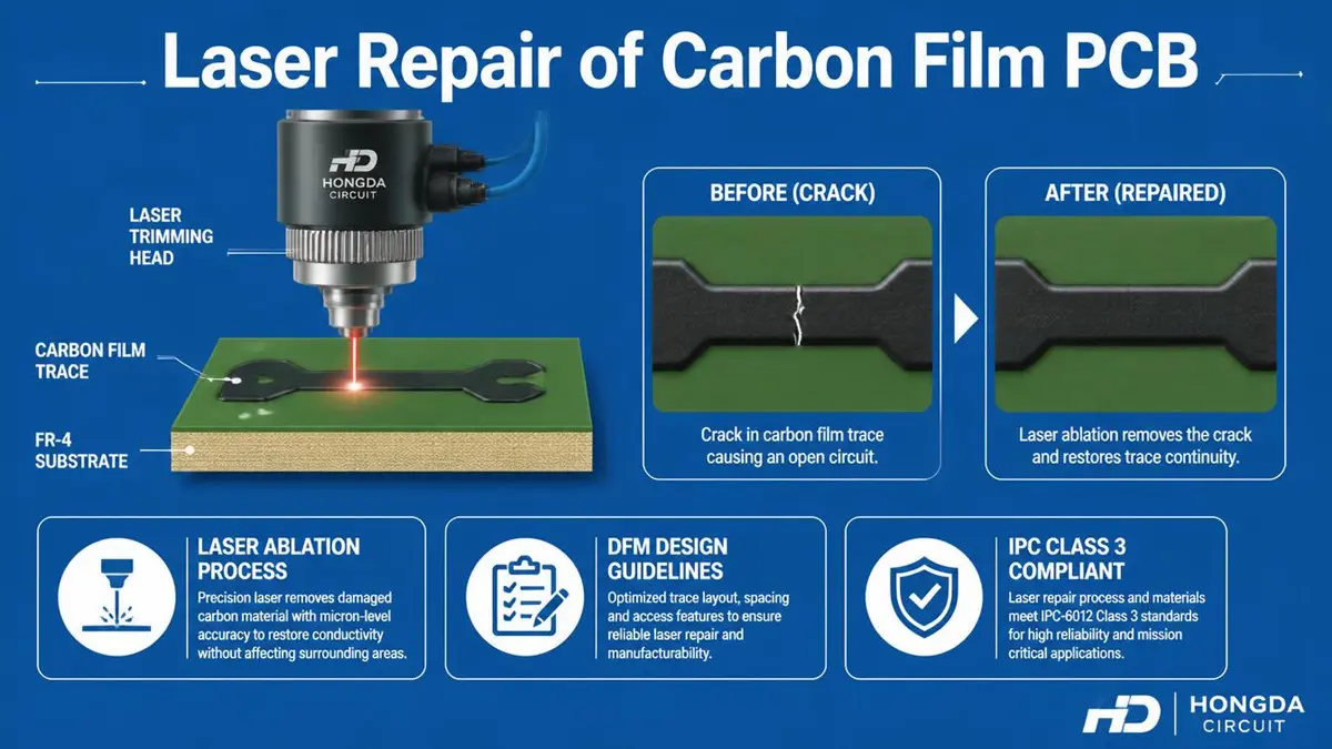
Laser Repair of Carbon Film PCB – Hongda Circuit
Screen printing is the industry workhorse for carbon film PCBs: 100–200 mesh screens deposit a 10–30 µm wet film, followed by curing at 140–160 °C for 15–30 minutes, or a UV flash plus 80 °C bake. Automated lines reach 1,000+ panels per hour, making this the lowest-cost option at volume.
Inkjet printing suits prototypes and fine features: 1–10 µm layer thickness, low-viscosity inks (<20 cP), 20–50 µm line resolution, with UV or thermal curing. Throughput is far lower than screen printing.
Aerosol jet enables 5–50 µm non-contact deposition on planar or mildly 3D surfaces — useful for conformal contact elements.
Laser ablation and laser trimming remove material with 20–100 µm kerf for cutting custom trace patterns or trimming printed resistors to ±5% without a photomask.
Process details that separate good suppliers from average ones:
Substrate pretreatment: a 50–200 W oxygen plasma treatment for 1–5 minutes typically lifts cross-hatch adhesion from 3B to 5B on ASTM D3359. Pre-bake FR-4 at 100–120 °C to outgas moisture before printing.
Substrate compatibility: FR-4, polyimide (Kapton), and PET flex films are all standard; cure temperatures above 150 °C exclude PET.
Throughput vs. resolution: specify your feature size first — it determines the deposition method and the stencil/tooling cost.
Design Guidelines and DFM for Carbon Contact Pads and Traces
Design rules that keep carbon film PCBs manufacturable and reliable:
Feature sizes: plan for 0.15–0.20 mm (6–8 mil) minimum trace width and spacing for screen printing. Oversize carbon contact pads by 0.3–0.5 mm versus the copper land to tolerate registration tolerance.
Pad geometry: use round or oval pads for rubber-dome and metal-dome contacts; avoid sharp corners that concentrate wear.
Layer handling: put carbon features on a separate Gerber layer (e.g., named CARBON or .GCO) and call out the layer stack-up in the fabrication notes. Do not cover carbon contact areas with solder mask — carbon is the final surface finish there.
Isolation from solder zones: keep carbon elements at least 0.25 mm from copper solder lands. Carbon ink is not solderable, and flux residue degrades contact surfaces.
Mixed finishes: combine freely with ENIG, OSP, or HASL boards — just zone them so plated pads carry the solder joints and carbon carries the sliding or pressing contacts.
Quantify wear up front: specify actuation life (≥1,000,000 cycles for keypads), contact force range (100–300 g), and stroke parameters, referencing ASTM D4060 (Taber abrasion, CS-10 wheel, 1 kg load) for sliding elements.
DFM checklist for your review: carbon layer present and named; pad oversize applied; solder mask clearance around carbon zones; sheet resistance target with thickness; adhesion class 5B; wear test conditions; carbon-to-copper isolation distance.
Assembly, Solderability, Repair, and Rework
Carbon film is not directly solderable: the resistive surface does not wet with tin-lead or SAC alloys, and flux burns permanently degrade contact pads. Plan your assembly flow accordingly.
Recommended attachment methods:
Silver-filled conductive epoxy (ECA): two-part adhesives cured at 100–150 °C for 30–60 minutes (or 24 h at room temperature) achieve 5–50 mΩ joint resistance. This is the default for attaching components to carbon pads.
Crimp and press-fit terminations for connectors onto carbon-plated pads.
Plated over-coat: where a true solder joint is mandatory, suppliers can electroless-plate nickel (3–5 µm) and gold (0.05–0.1 µm) over carbon — a special process that requires plasma pretreatment and adds cost and lead time.
Process recommendations:
Ensure carbon ink is fully cured before reflow; a typical lead-free profile (preheat 150–180 °C, 60–90 s above 217 °C, peak 245–255 °C) is tolerated well, but outgassing from under-cured ink causes blistering and adhesion loss.
During wave soldering, mask or bottom-side carbon features to prevent flux contamination.
Rework conductive-epoxy joints with localized heat (~150 °C) and solvent cleaning; do not scrape carbon pads.
Repair options: bridge opens with a silver-epoxy dot (re-test sheet resistance afterward); laser-trim out-of-tolerance resistors (typically ±5% achievable); locally metalize worn contact pads with electroless Ni/Au. Each repair is a documented risk — track them in your DPMO statistics, since reworked joints are the most common early-life failure site.
Testing, Reliability, Applications, and Cost Considerations
Electrical and mechanical test plan:
Sheet resistance: four-point-probe mapping on a 10 mm grid; require mean ± 1σ reporting per ASTM F390/F84.
Adhesion: ASTM D3359 cross-hatch (1 mm grid, 3M 610 tape) — require Class 5B, no flakes.
Abrasion: ASTM D4060 Taber testing for sliding contacts; specify wheel, load, and cycle count (e.g., 1,000 cycles at 1 kg).
Environmental: thermal shock −40 °C to +85 °C, 100 cycles (IEC 60068-2-14 / MIL-STD-202 Method 107); damp heat 85 °C/85% RH for 500–1,000 h (IEC 60068-2-78); salt fog 48–96 h (ASTM B117) for exposed-contact designs.
Pass criteria: sheet resistance shift <10%, contact resistance change <20%, adhesion ≥4B, no cracking after cycling.
Typical US-market applications: consumer membrane-switch keypads, automotive interior buttons and seat/steering-wheel controls, medical device sensors and disposable electrode contacts, industrial potentiometers and encoders, printed RFID antennas, low-power heater elements, and EMI contact pads.
Cost picture: carbon ink is dramatically cheaper than silver — material cost for a typical keypad pad set is a fraction of a cent versus $0.05–0.20 for an equivalent silver-ink area. Screen-print tooling is a one-time $50–$300 stencil charge, ideal for prototypes and low volume (US quick-turn shops deliver 5–10 day turns at $100–$500 NRE). For long, high-current traces, silver’s lower resistance reduces power loss and may justify its premium in the lifecycle cost model. For short contacts, resistors, and wear elements, carbon wins on both piece price and durability.
Get a Quote for Your Carbon Film PCB
Send us your Gerber files (including the dedicated carbon layer), target sheet resistance, and required test plan — we will return a prototype quote in 24 hours, with 5-day quick-turn production in the US. Options include:
Free sample kit with measured sheet-resistance, adhesion (ASTM D3359), and thermal-cycling data
Specified IPC/ASTM test reporting — four-probe mapping, cross-hatch, Taber abrasion, and 85/85 damp heat
Low-volume prototype pricing from 5 pieces, no hard-tooling charges for screen-printed designs
All products are RoHS- and REACH-compliant, with UL 94 V-0 laminates and UL 796 recognition available. US customers: state your UL file or flame-rating requirements on the RFQ so we can certify the correct construction. The fastest evaluations come from RFQs that include a measurable data package — include your sheet-resistance window, adhesion class, and cycle-life target, and our engineers will review the design for DFM issues before quoting.
FAQ
What is the typical sheet resistance range of carbon film PCBs and how is it specified?
Standard carbon inks measure 15–100 Ω/sq at 10–25 µm cured thickness; high-resistance formulations reach 1,000+ Ω/sq. Always specify sheet resistance together with cured thickness and test method (ASTM F390/F84 four-point probe).
Can you solder directly to carbon film contact pads, and what assembly techniques are recommended?
No — carbon is not solderable. Use silver-filled conductive epoxy, crimp, or press-fit terminations. If soldering is mandatory, pads can be electroless-plated with nickel/gold as a special process.
Which deposition methods are best for high-resolution carbon traces?
Inkjet (20–50 µm lines) and aerosol jet (5–50 µm) offer the finest resolution; screen printing is limited to roughly 150–200 µm features. Laser ablation trims features after printing without a mask.
How is adhesion of carbon ink to FR-4 measured, and what treatments improve bonding?
Via ASTM D3359 cross-hatch tape testing; Class 5B is required. Oxygen plasma treatment (1–5 min, 50–200 W) and a 100–120 °C substrate pre-bake improve adhesion from 3B to 5B.
What environmental and reliability tests should I require for automotive or medical carbon film PCBs?
Require thermal shock −40/+85 °C (100 cycles, IEC 60068-2-14), damp heat 85 °C/85% RH (500–1,000 h, IEC 60068-2-78), ASTM D3359 adhesion ≥4B, Taber abrasion per ASTM D4060, and IPC-6012 Class 3 qualification for medical or safety-critical use.
How do repair and rework methods for carbon films compare in durability and ease of implementation?
Silver-epoxy dot repairs are easy but must be re-tested electrically; laser trimming suits resistors (±5%); electroless Ni/Au re-metalization of worn pads is the most durable but costliest. Reworked joints carry higher early-failure risk and should be logged.
How do lifecycle costs compare between carbon film, copper traces, and silver conductive inks for low-volume production? Carbon wins on material cost and wear life for contacts, resistors, and short traces, with low stencil NRE. Silver suits long or high-current runs where its 0.005–0.05 Ω/sq sheet resistance saves energy. Copper remains the default for standard circuitry; carbon typically supplements it as a functional surface layer.
About Author
David Chen https://www.linkedin.com/in/pcbcoming
David Chen is a Senior RF/PCB Process Engineer at Shenzhen Hongda Circuit Technology Co., Ltd., with over 12 years of experience in high-frequency PCB fabrication, impedance-controlled stack-up design, and Rogers/PTFE laminate processing. He also boasts an extensive professional background in PCBA manufacturing, PCBA testing, and PCBA optimization, with specialized expertise in high-precision PCBA fault analysis and rigorous PCBA reliability testing. The author has worked with high-layer-count server PCB fabrication, ultra-low-loss backplane stackups, and thermo-mechanical reliability optimization for AI infrastructure projects involving 112G and 224G PAM4 architectures. Skilled in complex circuit design and cutting-edge advanced PCB manufacturing processes, he delivers solutions that elevate product durability and performance across industrial applications. His technical articles focusing on PCBA manufacturing workflows and testing methodologies are widely cited by industry peers and technical platforms, and have gained attention and recognition from industry colleagues.