PCB burst plate reflow soldering defects are common and costly issues faced by quality, procurement and process engineers within electronics manufacturing. This article covers defect classification, step‑by‑step failure diagnosis, material & storage controls, reflow oven tuning, and closed‑loop corrective‑action best practices aligned with IPC / J‑STD industry standards.
Many engineers recognise “burst plate” as a direct translation from Chinese industry jargon. In global PCB manufacturing environments, this failure phenomenon overlaps with well‑known terminology including blistering, delamination, popcorning, and measling. Misused terminology often sends root‑cause investigation down incorrect paths, making clear classification critical for cross‑factory and supplier‑buyer alignment.
What Is a Burst‑Plate Defect in PCB Reflow: Defect Modes and Classification
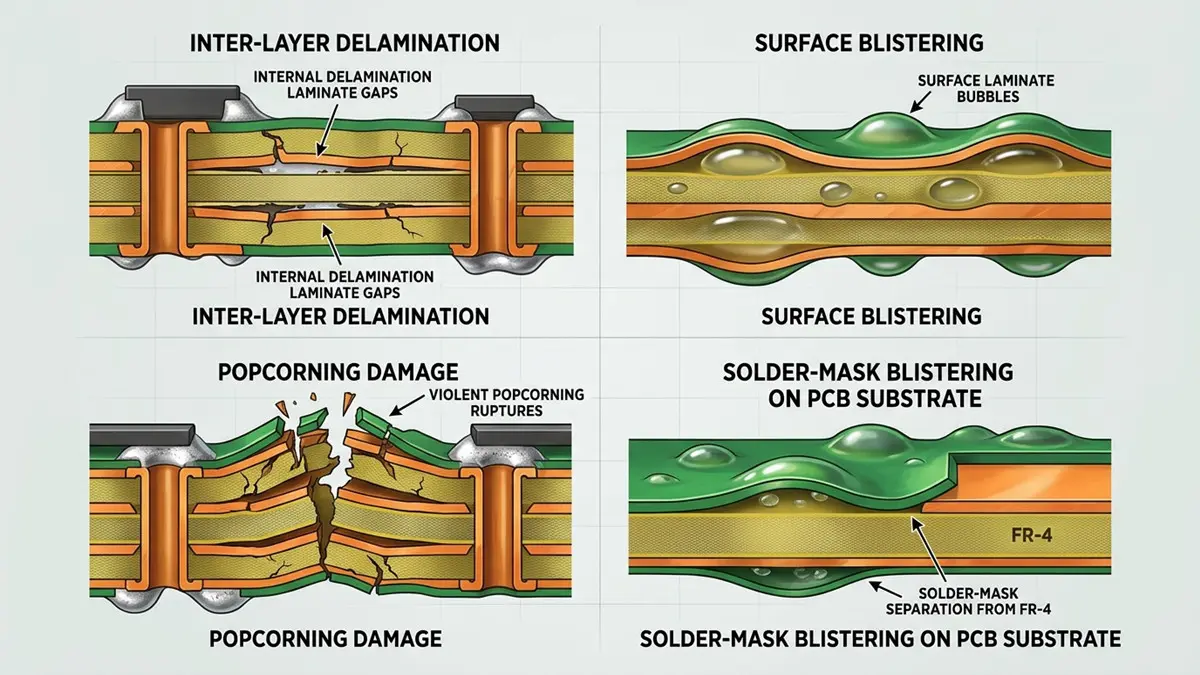
A burst‑plate defect describes localised delamination, blistering, bulging or catastrophic substrate cracking triggered by combined internal mechanical stress and trapped gas expansion when PCBs experience high reflow temperatures. This condition must be distinguished from intentional structural features such as pressure‑relief channels.
Four core failure modes are frequently observed:
- Inter‑layer delamination: physical separation between laminate layers
- Surface blistering: local raised bulges on board or solder‑mask surfaces
- Popcorning failure: violent rapid expansion of entrapped moisture vapour
- Solder‑mask blistering: bubbling isolated to the outer protective mask layer
Each mode carries distinct root causes, visual appearances, and typical board‑level occurrence locations.
Engineers must also watch for secondary associated damage that often remains partially hidden under intact surfaces: solder wicking, internal voiding, copper‑foil‑to‑substrate separation, and plated‑through‑hole wall cracking. Surface bulging is frequently only the visible symptom of extensive internal substrate degradation.
Clear acceptance criteria set the baseline for all subsequent analysis and corrective work. Different product reliability grades define allowable limits for delamination area and defect placement. Without aligned acceptance rules between PCB purchasers, contract assemblers, and component suppliers, improvement efforts lack consistent pass‑fail benchmarks.
Root‑Cause Diagnosis Workflow: From Visual Inspection to SEM/EDS
Effective burst‑plate troubleshooting follows a structured sequence: non‑destructive testing first, then destructive analysis; confirm defect layer position before pinpointing driving failure mechanisms.
- Start with visual and low‑magnification microscopic documentation. Record defect size, location, and whether failures cluster along copper‑foil edges or around plated holes.
- Deploy acoustic scanning, X‑ray or micro‑CT scanning to map delamination depth and detect subsurface voids without ruining physical samples.
- Prepare targeted cross‑section metallographic samples to examine resin‑glass‑fibre interfaces, copper‑foil surface residues, and plated hole‑wall integrity.
- Where needed, run SEM‑EDS to identify contaminant elemental signatures; use ion‑chromatography testing to quantify ionic residue levels.
Two practical, often‑overlooked points heavily impact test reliability:
- Correct sample selection and proper sample storage to prevent secondary damage after failure occurs
- Grinding orientation during cross‑section preparation, which can easily distort interpretation of interfacial damage
Learn to read test outputs correctly: specific morphological features indicate moisture‑driven popcorning damage; other signatures point toward thermal shock or CTE‑mismatch stress. Test evidence differentiates defects originating from incoming raw‑material quality versus process‑induced contamination during assembly.
Use a printable production‑floor troubleshooting checklist, organised into three columns: observed phenomenon, required verification action, and corresponding diagnostic conclusion. Quality and procurement teams can deploy this tool immediately for incoming‑part quality disputes between buyers and PCB vendors.
Moisture, Laminate Selection, and Storage Controls That Prevent Burst‑Plate Events
Material performance and moisture exposure are inseparable contributors to burst‑plate risk, and must be managed as one unified control domain.
Moisture accumulates along resin‑glass‑fibre boundaries under humid ambient conditions. During reflow heating, trapped moisture instantly vaporises; when steam pressure exceeds inter‑layer bonding strength, delamination and bursting occur.
Follow formal moisture‑sensitivity management governed by industry standards J‑STD‑020 and J‑STD‑033:
- Enforce traceable records for dry‑pack incoming‑PCB unpacking and temperature acclimatisation
- Monitor factory floor‑life exposure duration
- Apply qualified baking profiles for PCBs that exceed permitted ambient exposure windows — avoid generic “bake the boards” guidance without specification
Laminate material selection requires quantitative parameter evaluation: glass‑transition temperature (Tg), decomposition temperature (Td), Z‑axis coefficient of thermal expansion (CTE‑Z), and copper‑foil peel strength.
- High‑Tg laminates deliver improved resistance under multiple reflow cycles yet introduce trade‑offs in cost and manufacturability
- Calculate thermal safety margins specifically for high‑temperature lead‑free assembly processes
- Match resin plugging performance and prepreg material grades to maintain robust inter‑layer adhesion
Ambient climate creates real‑world variability across global manufacturing sites. High‑humidity summer conditions in the US Southeast and Gulf Coast produce vastly different moisture‑absorption risks compared with dry south‑western US facilities, even for identical PCB stock. Procurement and manufacturing teams must embed dehumidified warehousing rules and environmental controls aligned with ANSI/ESD S20.20 within formal work instructions.
Use a three‑phase checklist covering incoming‑material inspection, controlled warehousing, and pre‑reflow pre‑treatment to consolidate these controls for supplier and internal‑process compliance reviews.
Reflow Profile and Oven Optimisation: Ramp, Soak, Peak, and Cooling
Even with well‑specified incoming PCB materials, poorly optimised reflow oven settings will trigger burst‑plate failures. A widespread field mistake is copying solder‑paste supplier reference profiles directly without performing real‑board thermal measurement.
Attach thermocouples at multiple representative locations: board surfaces, panel edges, large copper‑land areas, and high‑density via clusters. Capture true thermal differentials across the assembled PCB panel and tune oven parameters based on measured board temperatures instead of oven set‑point values.
Key reflow zone tuning guidelines
- Pre‑heat / Ramp: Keep ramp rates below 2 °C per second to minimise thermal shock
- Soak segment: Adequate soak time activates flux chemistry while equalising panel temperature distribution; insufficient soak amplifies internal board temperature gradients
- Peak temperature & Time‑Above‑Liquidus: Define total thermal load applied to PCB resin systems. Where solder joint quality permits, operate peak thermal conditions toward the lower end of acceptable operating windows to reduce substrate heat stress
- Cooling: Excessively fast cooling introduces additional thermal stress capable of initiating hidden substrate cracking
Equipment‑level tuning includes balanced temperature‑zone configuration, matching conveyor chain speed to thermal requirements, and evaluating nitrogen‑atmosphere benefits for joint wetting and oxidation reduction.
Important: Whenever solder‑paste formulations, PCB laminate lots, or fixture carriers change, re‑validate the full thermal profile.
Quick shop‑floor screening rule: Significant temperature deviation between measurement points on one identical panel indicates oven drift or fixture‑related thermal problems, enabling preliminary assessment without laboratory‑grade analysis equipment.
Preventing Recurrence: Design Rules, Corrective‑Action Plans, and Validated Improvement
Once root causes are confirmed, cross‑functional teams must implement sustainable recurrence‑prevention solutions covering hardware design, formal corrective actions, and verified process improvement.
At the design phase, mitigate burst‑plate risk by:
- Tuning via and pad geometries
- Managing thermal gradients around dense‑via zones
- Qualifying resin‑plug processes
- Adding buffer structures in zones with large copper areas prone to CTE‑mismatch stress
Each mitigation carries trade‑offs; select preferred solutions based on your product category rather than applying universal design rules without context.
Establish closed‑loop corrective‑action tracking:
- Document remediation steps with clear responsible parties, defined verification methods, and objective pass‑fail acceptance criteria
- Use Design‑of‑Experiments (DOE) methodology to isolate dominant influencing factors instead of relying on trial‑and‑error adjustments
- Lock critical process parameters within statistical‑process‑control (SPC) limits after optimisation
- Validate improvement via first‑article confirmation plus reliability testing: thermal‑cycle exposure and simulated multiple reflow cycles
- Conduct supplier‑side process audits to suppress incoming‑material variability at source
Quantify business impact: consistently measure pre‑ and post‑improvement defect rates, scrap volume, and rework expenses to demonstrate return‑on‑investment.
Support quality and procurement workflows with reusable templates: a failure‑analysis‑report outline and cross‑department corrective‑action tracking spreadsheet fields for direct reuse by your quality and supply‑chain teams.
Next Steps & Technical Support
Stop repeating costly PCB‑assembly scrap caused by reflow‑induced burst‑plate, blistering and delamination failures.
Download free resources: Burst‑plate troubleshooting checklist, reflow‑profile‑validation log sheet, editable failure‑analysis‑report template.
We offer a complimentary one‑time process review or sample‑level failure analysis for North‑American customers. Our team supports quick‑turn prototyping, production‑ramp‑up challenges, and high‑reliability automotive and industrial electronics subject to strict IPC‑aligned acceptance standards.
Our technical specialists speak directly to procurement‑quality and customer‑quality requirements, helping you minimise scrap batches and shorten corrective‑action timelines. Submit your defect photographs, process records and PCB specifications to open your technical support request today.
Frequently Asked Questions
Q1: What is a “burst‑plate” defect in PCB reflow, and how is it different from blistering and delamination?
Burst‑plate” comes from Chinese manufacturing jargon, describing substrate cracking, bulging or layer separation triggered by heat and internal gas pressure during reflow. Blistering refers to local raised surface bubbles, while delamination means separation between internal PCB laminate layers. Popcorning specifically describes violent damage caused by fast vaporisation of trapped moisture. One visible surface symptom can hide multiple internal failure modes, so clear terminology is critical for supplier‑buyer quality negotiations.
Q2: What actually causes PCBs to burst or blister during reflow soldering?
Three major root‑cause categories drive these failures: moisture absorption of the PCB laminate, material property gaps (such as insufficient Tg, Td or poor Z‑axis CTE performance), and assembly‑process issues including excessive thermal shock from misconfigured reflow profiles. Design layout risks like dense via clusters or large copper planes can amplify stress and make defects more likely to occur. In many real‑world cases, two or more of these factors work together to trigger failure.
Q3: my PCB reflow blister / burst‑plate failure?
Start with non‑destructive checks such as acoustic scanning and X‑ray CT. Metallographic cross‑section combined with SEM‑EDS testing delivers definitive evidence. Moisture‑related popcorning damage typically shows clean resin‑fibre interface separation. CTE‑mismatch failures tend to appear near heavy copper, vias or board edges, with mechanical‑stress‑driven crack propagation. Site history also helps: if failures rise after high‑humidity warehouse seasons, moisture is highly suspect.
Do I need to bake PCBs before reflow, and what baking schedule should I follow?
Pre‑reflow baking is mandatory for PCBs that have exceeded their allowed factory floor‑life after dry‑bag opening. Always follow J‑STD‑020 and J‑STD‑033 standards. Baking temperature, hold‑time and post‑bake dry‑storage rules change based on laminate material, PCB thickness and exposure duration. Generic “one‑size‑fits‑all” baking settings risk over‑baking and further degrade inter‑layer adhesion. Your procurement and quality teams should lock qualified baking profiles into supplier specifications.
Which industry standards define acceptable limits for PCB delamination and blistering?
IPC‑A‑600 sets visual acceptance criteria for PCB end‑products, covering maximum allowable delamination area, depth and location. IPC‑6012 specifies performance requirements for rigid printed‑boards by product reliability class (commercial, industrial, automotive high‑reliability). J‑STD‑020 / J‑STD‑033 govern moisture‑sensitivity handling for assembly. Procurement contracts should reference exact revision levels of these standards to eliminate ambiguous pass‑fail judgement between buyers and PCB vendors.
How should I adjust my reflow profile to stop burst‑plate failures?
Never directly reuse solder‑paste supplier reference curves without real‑board thermocouple measurement. Control pre‑heat ramp rate ≤ 2 °C/s to reduce thermal shock. Optimise soak time for uniform board temperature. Set peak temperature and time‑above‑liquidus to the minimum acceptable window that still guarantees good solder joint quality. Avoid overly fast cooling rates. Remember: after changing PCB lots, solder paste or oven fixtures, you must re‑validate the full thermal profile.
How can I objectively prove corrective actions have fixed my burst‑plate problem?
Visual inspection alone is insufficient. Build a validation package including: pre‑vs‑post defect scrap‑rate statistics, DOE test results, updated SPC process control charts, first‑article cross‑section analysis, and reliability testing such as repeated simulated reflow cycles or thermal cycling tests. Retain traceable production records. For procurement purposes, require your PCB or assembly supplier to submit complete objective evidence rather than verbal confirmation of improvement.
About Author
David Chen LinkedIn Profile
David Chen is a Senior RF/PCB Process Engineer at Shenzhen Hongda Circuit Technology Co., Ltd., with over 12 years of experience in high-frequency PCB fabrication, impedance-controlled stack-up design, and Rogers/PTFE laminate processing. He also boasts an extensive professional background in PCBA manufacturing, PCBA testing, and PCBA optimization, with specialized expertise in high-precision PCBA fault analysis and rigorous PCBA reliability testing. The author has worked with high-layer-count server PCB fabrication, ultra-low-loss backplane stackups, and thermo-mechanical reliability optimization for AI infrastructure projects involving 112G and 224G PAM4 architectures. Skilled in complex circuit design and cutting-edge advanced PCB manufacturing processes, he delivers solutions that elevate product durability and performance across industrial applications. His technical articles focusing on PCBA manufacturing workflows and testing methodologies are widely cited by industry peers and technical platforms, and have gained attention and recognition from industry colleagues.