In the fast-paced world of hardware development, knowing how to reduce high-frequency PCB fabrication lead time for urgent projects can mean the difference between a successful market launch and a missed opportunity. High-frequency printed circuit boards—essential for 5G telecommunications, aerospace radar, and AI infrastructure—require specialized materials and high-precision manufacturing. When project timelines shrink, engineering teams must optimize every stage of the design and fabrication pipeline to eliminate bottlenecks without compromising signal integrity.
The Core Challenge: Why High-Frequency PCBs Face Production Delays
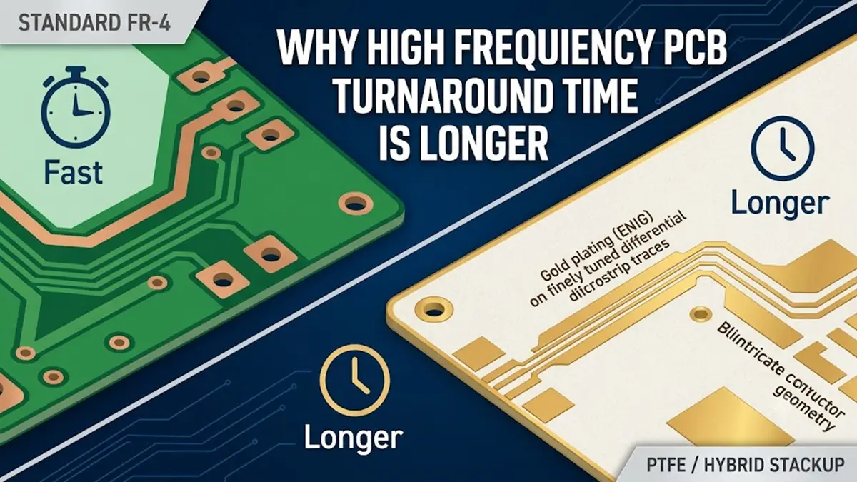
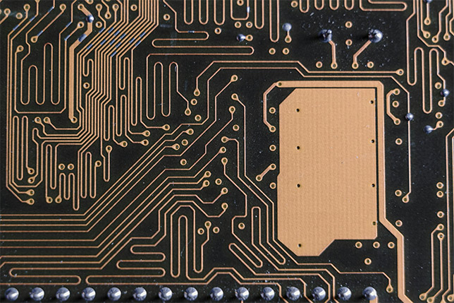
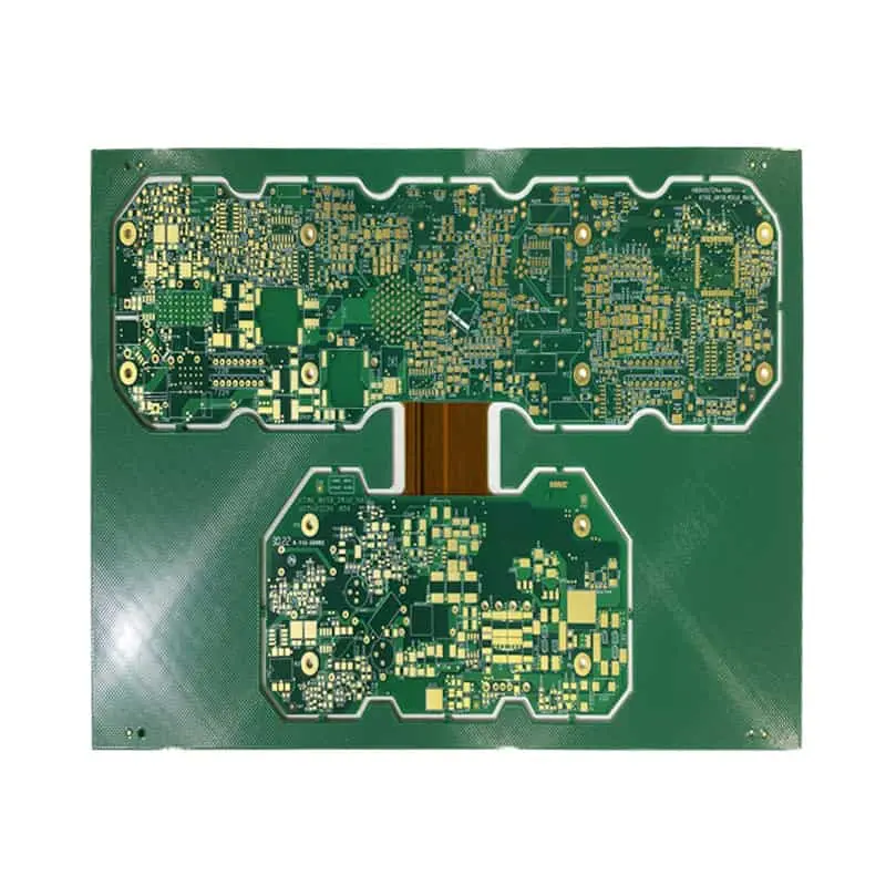
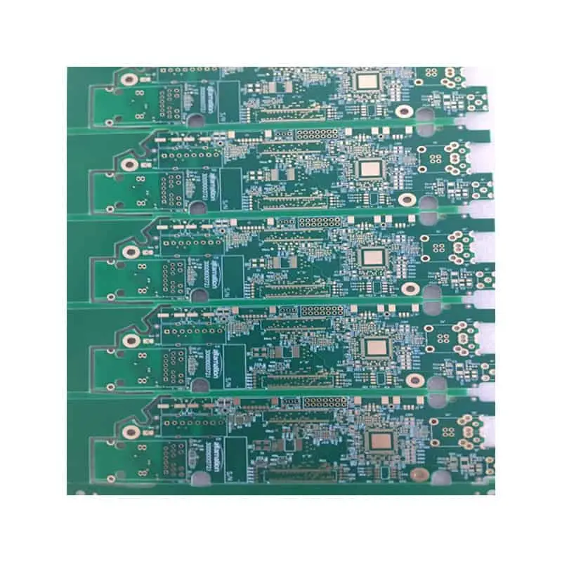
High-frequency boards operate at gigahertz (GHz) frequencies where signal loss and impedance mismatch can ruin a design. Consequently, fabricating these boards takes longer than standard FR-4 manufacturing due to strict material handling requirements, precise registration needs, and specialized surface finishes.
The Fast-Track Matrix: Standard vs. Accelerated Processing
To understand where time can be saved, consider how an expedited manufacturing workflow compresses the traditional timeline:
| Fabrication Phase | Standard Lead Time | Expedited Lead Time (Urgent Projects) | Critical Acceleration Leverage Point |
| DFM Review & CAM | 24 – 48 Hours | 2 – 4 Hours | Pre-validated design files & active engineering collaboration. |
| Material Sourcing | 3 – 10 Days | 0 Days (In-Stock) | Specifying locally inventoried, high-frequency laminates. |
| Lamination & Drilling | 48 – 72 Hours | 12 – 24 Hours | Controlled depth drilling and sequential lamination optimization. |
| Surface Finishing | 24 Hours | 4 – 8 Hours | Selecting finishes with high throughput and low lead times. |
| Final Inspection & Flying Probe | 24 Hours | 4 – 6 Hours | Designing dedicated test points for automated parallel testing. |
3 Strategic Pillars to Accelerate High-Frequency PCB Turnaround
1. Optimize Design for Manufacturing (DFM) Specifically for High Frequency
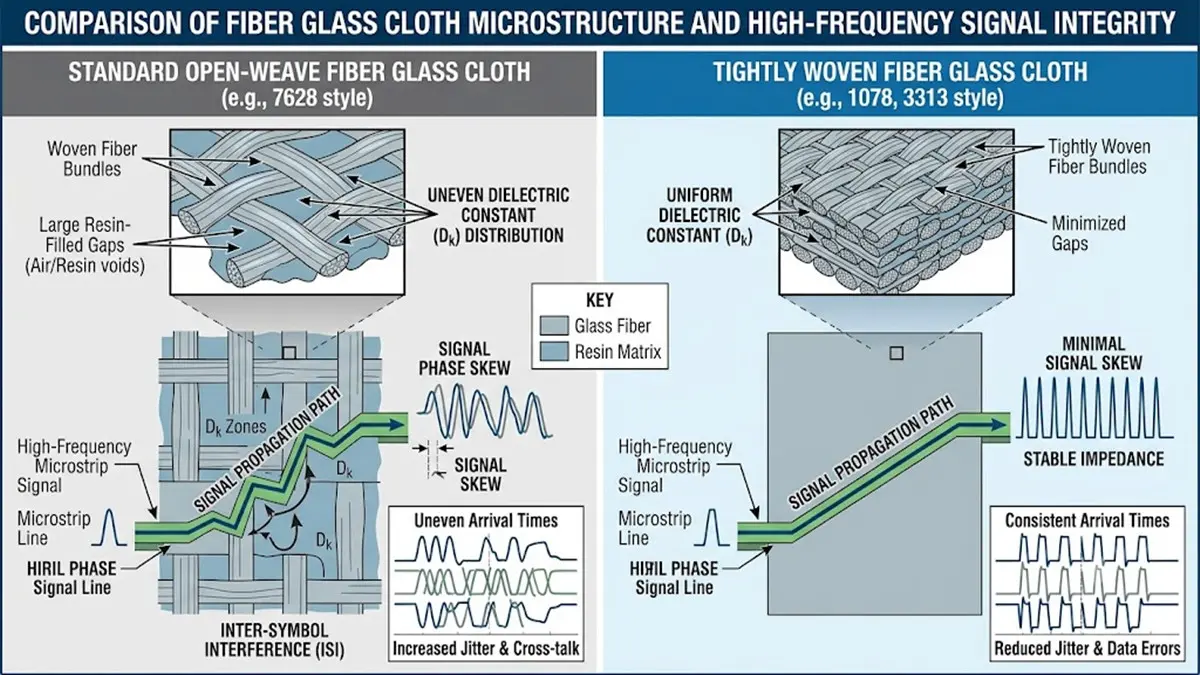
Impact of Glass Fiber Weave Styles (Open-Weave vs. Tightly Woven) on High-Speed Signal Integrity and Phase Skew.
The most common cause of fabrication delay is the “engineering query” (EQ) loop, where the manufacturer pauses production to clarify ambiguous design details.
Standardize Stackup Configurations Early: Do not design a complex multi-layer stackup in isolation. Request the fabricator’s exact material datasheets (e.g., Rogers, Taconic, or Panasonic Megtron series) before routing.
Account for Copper Weave and Fiber Splay: High-frequency signals are sensitive to the glass weave effect. Work with a manufacturer who keeps tightly woven glass styles (like 1078 or 3313) in stock to avoid specialized ordering delays.
Provide Flawless ODB++ or Gerber X2 Files: Traditional Gerber RS-274X files often require manual netlist generation and layer verification. Moving to modern formats like ODB++ eliminates data ambiguity, cutting CAM processing time by up to 70%.
2. Strategic Material Selection and Pre-Ordering Logistics
Material availability is the single largest bottleneck in high-frequency fabrication. Specialty PTFE (Teflon) and thermoset hydrocarbon laminates are rarely commodity items.
BOFU Decision Tip: When speed is paramount, ask your manufacturer: “What high-frequency laminates do you currently hold in your immediate, climate-controlled inventory?” Designing your board around an in-stock Rogers 4003C or 4350B laminate can shave up to 7 business days off your total lead time compared to ordering an exotic, non-stock material.
3. Streamline Panelization and Mechanical Constraints
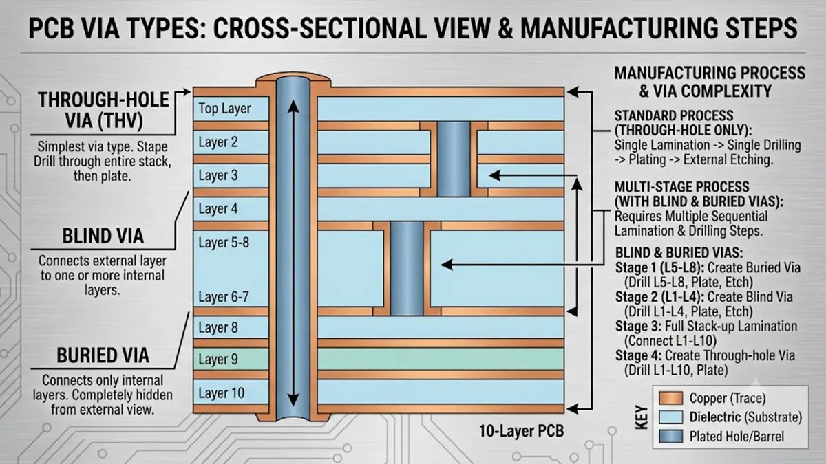
Cross-Sectional Comparison of Through-Hole, Blind, and Buried Vias with Multi-Stage Manufacturing Workflow.
Complex mechanical routing slows down CNC machining lines. To keep fabrication moving fast:
Keep board shapes as rectangular as possible to allow rapid V-scoring rather than tedious tab-routing.
Minimize the use of blind and buried vias unless absolutely necessary for routing density. Every extra lamination cycle adds at least 12 to 18 hours to the production floor timeline.
Real-World Case Study: Accelerating a 24GHz Radar PCB Project
The Challenge
A tier-one automotive radar client needed a prototype batch of ten 6-layer hybrid PCBs (utilizing Rogers RO4350B bonded to standard FR-4 cores) for an upcoming compliance audit. The standard quoted lead time was 12 business days, but the client needed them shipped within 4 business days.
The Solution
The engineering team initiated a pre-layout consultation with the factory CAM department. By implementing the following three steps, the project was fast-tracked:
Live DFM Collaboration: The client’s layout engineers worked concurrently with the fabrication team via a shared cloud environment to resolve impedance line-width variations in real-time.
In-Stock Inventory Lock: The board design was explicitly adapted to match the precise copper foil thickness (0.5 oz) and core thickness (10 mil) available on the factory floor that morning.
Parallel E-Testing: The panel design was optimized to allow multi-headed flying probe testing to occur simultaneously, slashing final QC time.
The Results
Total Engineering Queries: Reduced from an average of 5 down to 0.
Total Fabrication Lead Time: Successfully compressed from 12 days to 3.5 days.
Signal Integrity Retention: Post-fabrication insertion loss testing showed 100% adherence to the target $0.12\text{ dB/cm}$ limit at 24GHz.
Deep-Dive FAQ: Mid-to-Late Stage Engineering Insights (MOFU/BOFU)
Q1: How does material selection directly impact how to reduce high frequency PCB fabrication lead time for urgent projects?
Material availability is the single largest bottleneck in quick-turn production. Standard FR-4 laminates are always in stock, but specialized high-frequency laminates often require custom ordering if your specific thickness or copper weight isn’t on the floor.
To drastically reduce lead time for urgent projects, engineers should consult their fabricator before finalizing the schematic. Designing your stackup around the manufacturer’s immediate, in-stock climate-controlled inventory can eliminate up to 5 to 7 days of external material sourcing transit time.
Q2: Which surface finish should be specified to maintain signal integrity while minimizing quick-turn PCB manufacturing delays?
When figuring out how to reduce high frequency PCB fabrication lead time for urgent projects, surface finish processing time plays a critical role. Electroless Nickel Immersion Gold (ENIG) is highly reliable but involves a complex, multi-step chemical plating process that adds hours to production. Furthermore, the nickel layer can introduce insertion loss at frequencies above 10 GHz due to the skin effect.
For high-frequency boards on tight deadlines, specifying Immersion Silver (ImAg) or Organic Solderability Preservatives (OSP) is highly recommended. These finishes offer a perfectly flat surface for fine-pitch components, provide superior signal performance at high frequencies, and feature significantly shorter processing lines on the factory floor, saving 4 to 8 hours of manufacturing time.
Q3: What is the fastest format to submit design data when looking at how to reduce high frequency PCB fabrication lead time for urgent projects?
The fastest and most reliable format to submit is ODB++ or Gerber X2. Traditional Gerber RS-274X files are prone to data ambiguity because they require separate files for drills, netlists, and layer stackup definitions, which often forces CAM engineers to halt production to raise an Engineering Query (EQ).
By upgrading your export format to ODB++, you provide the fabricator with a unified, intelligent data structure that includes netlists, stackups, and components in a single file. This eliminates manual data reconstruction and can compress the initial CAM validation and DFM review phase from 24 hours down to less than 2 hours.
Q4: How can modifying via designs and layer stackups help reduce rapid-turnaround microwave PCB production bottlenecks?
The mechanical complexity of your board dictates how fast it moves through the automated drilling and lamination lines. If you want to know how to reduce high frequency PCB fabrication lead time for urgent projects, you should minimize or eliminate blind and buried vias unless they are structurally mandatory for your routing density.
Every set of blind or buried vias requires an independent sequential lamination cycle and separate controlled-depth drilling runs. A single extra lamination cycle adds at least 12 to 18 hours of processing and baking time. Keeping your design to a single-press multi-layer stackup with standard through-hole vias is one of the most effective ways to keep production on the fast track.
Q5: Why is a pre-layout DFM consultation crucial when planning how to reduce high frequency PCB fabrication lead time for urgent projects?
The primary cause of delays in expedited manufacturing is not the speed of the machinery, but communication friction. Up to 30% of high-frequency PCB designs encounter an impedance or registration conflict during the CAM review, which completely stops the clock on an urgent project.
A pre-layout Design for Manufacturing (DFM) consultation allows your engineering team to align trace widths and gap spacings directly with the fabricator’s precise chemical etching factors before the layout is finalized. Resolving these electrical and physical parameters proactively ensures your project skips the holding queue and goes straight into automated production the moment files are uploaded.
Conclusion: Partnering for Rapid Turnaround
Reducing high-frequency PCB fabrication lead time requires moving beyond a transactional relationship with your manufacturer. True acceleration happens when your engineering team treats the fabricator as an active partner early in the design cycle. By aligning your CAD layout directly with the factory’s real-time material inventory, utilizing modern manufacturing data formats, and resolving DFM considerations proactively, you can comfortably compress standard multi-week production timelines down to a matter of days.
When your next high-frequency project faces an aggressive deadline, implementing these strategic workflows will safeguard both your launch schedule and your high-frequency signal performance.
About Author
David Chen https://www.linkedin.com/in/pcbcoming
David Chen boasts an extensive professional background in PCBA manufacturing, PCBA testing, and PCBA optimization, with specialized expertise in high-precision PCBA fault analysis and rigorous PCBA reliability testing. The author has worked with high-layer-count server PCB fabrication, ultra-low-loss backplane stackups, and thermo-mechanical reliability optimization for AI infrastructure projects involving 112G and 224G PAM4 architectures. Skilled in complex circuit design and cutting-edge advanced PCB manufacturing processes, he delivers solutions that elevate product durability and performance across industrial applications. His technical articles focusing on PCBA manufacturing workflows and testing methodologies are widely cited by industry peers, research institutions, and technical platforms, solidifying his reputation as a recognized technical authority in the global circuit board manufacturing sector.