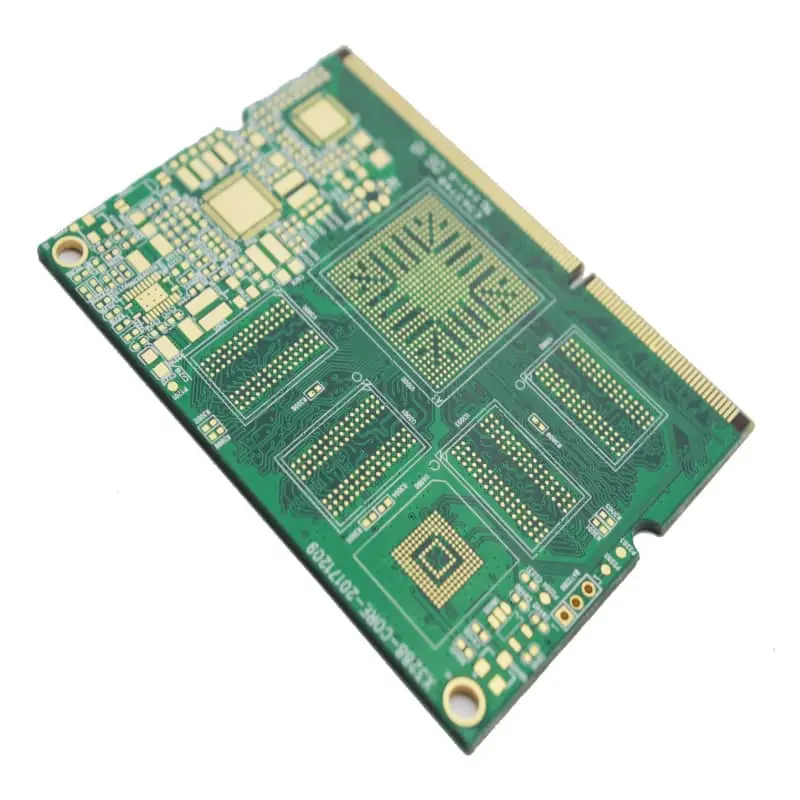
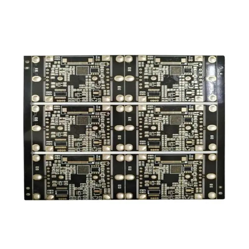
High frequency communication PCBs require controlled impedance, low-loss materials, short RF transitions, stable grounding, and tightly controlled fabrication. For 2.4 to 6 GHz wireless systems and higher-frequency microwave designs, the PCB stackup, copper geometry, dielectric properties, via structure, and connector transition must be engineered together rather than specified independently.
For OEMs and RF engineers sourcing a high frequency communication PCB, the critical procurement question is not simply whether a supplier can fabricate a multilayer board. The supplier must be able to translate the RF design into a manufacturable stackup, maintain controlled impedance through fabrication, and verify electrical performance with appropriate TDR and VNA measurements.
How should impedance control and layer stackup be optimized for high frequency communication PCBs?
Start with the target impedance, operating frequency, dielectric Dk and Df, finished dielectric thickness, copper thickness, and trace geometry. For many RF interfaces, 50 ohm single-ended and 90 to 100 ohm differential structures are common starting points. The final geometry should be verified with a field solver using the actual material construction proposed for production.
Example 50 ohm microstrip starting point
A practical 4-layer RF stackup can place the RF layer immediately above a continuous ground plane:
| Parameter | Example design value |
|---|---|
| RF layer | L1 |
| Reference plane | L2 GND |
| Dielectric height | 0.10 mm |
| Copper thickness | 35 um finished |
| Material | RO4350B-class laminate |
| Design Dk | Approximately 3.66 |
| Target impedance | 50 ohm |
| Initial trace width | Approximately 0.20 to 0.23 mm |
The exact trace width must be recalculated after the PCB fabricator confirms the pressed dielectric thickness, copper profile, solder mask condition, and material construction.
For a simplified microstrip calculation, impedance is primarily governed by the ratio between trace width and dielectric height and by effective permittivity:
Z0 = 60 / sqrt(Er_eff) * ln(8h / (w + t))This simplified expression is useful for understanding the relationship between geometry and impedance, but production RF designs should use an appropriate 2D electromagnetic field solver.
For example, if the dielectric height is reduced from 0.15 mm to 0.10 mm while copper thickness and material remain unchanged, the trace width normally needs to be reduced to maintain the same 50 ohm target. This is why a supplier should recalculate the stackup rather than copy a nominal trace width from another PCB.
For differential stripline, a typical starting construction may use 0.10 to 0.15 mm dielectric spacing to the reference planes, 18 to 35 um copper, and approximately 0.10 to 0.16 mm trace width with a controlled pair gap. A 100 ohm differential target should be confirmed with a field solver because pair spacing, copper thickness, glass weave, dielectric construction, and plane geometry all affect the final impedance.
How much impedance variation should be allowed?
The acceptable tolerance depends on the interface and system budget. A common PCB fabrication specification is plus or minus 10 percent impedance, while tighter RF and high-speed designs may specify plus or minus 5 percent when the complete link budget justifies the additional manufacturing control.
For example:
| Target | Typical tolerance example | Acceptable range |
|---|---|---|
| 50 ohm | +/- 10 percent | 45 to 55 ohm |
| 50 ohm | +/- 5 percent | 47.5 to 52.5 ohm |
| 100 ohm differential | +/- 10 percent | 90 to 110 ohm |
| 100 ohm differential | +/- 5 percent | 95 to 105 ohm |
These are specification examples rather than universal acceptance criteria.
At 2.4 GHz, a small geometric discontinuity may be more forgiving than the same discontinuity at 6 GHz or above. For procurement, specify the target impedance, tolerance, test method, stackup, dielectric thickness, copper thickness, and reference-plane definition together.
How should signal integrity, via transitions, and RF connectors be designed?
Keep RF paths short and continuous, minimize layer transitions, control via geometry, remove unnecessary stubs, and design the PCB-to-connector transition as part of the RF transmission line.
A high frequency communication PCB can lose performance even when the main RF trace has been calculated correctly. Common discontinuities include:
- Excessive via barrel length
- Large via pads
- Oversized or undersized anti-pads
- Long unused via stubs
- Abrupt trace-width changes
- Connector launch discontinuities
- Missing return-path stitching vias
- Ground-plane gaps underneath RF traces
For a layer transition, use a signal via with nearby ground vias to provide a low-inductance return path. The unused portion of the signal via should be minimized. Back-drilling becomes increasingly useful when the remaining stub becomes electrically significant.
As a practical first check, keep the residual via stub substantially below one tenth of the effective wavelength in the dielectric. Shorter stubs are preferable when return loss and insertion loss requirements are tight.
For SMA, SMB, board-to-coax, and similar launches, do not treat the connector as an independent mechanical component. The connector pad, anti-pad, signal via, ground vias, and transmission line should be designed and simulated as one electromagnetic structure.
A practical procurement requirement is:
Connector model, PCB stackup, launch geometry, and via structure should be reviewed together before prototype fabrication.
This helps prevent a common situation in which a PCB passes a basic impedance coupon test while the assembled RF port still shows excessive S11.
How can EMI, EMC, and grounding be controlled on a high frequency communication PCB?
Give high-frequency current a continuous, low-inductance return path before optimizing shielding or filtering.
A practical grounding sequence is:
- Establish an uninterrupted RF reference plane.
- Keep RF traces over the reference plane without crossing plane splits.
- Place decoupling capacitors immediately adjacent to IC power pins.
- Connect capacitor ground pads with short, low-inductance paths and nearby vias.
- Stitch ground planes around RF transitions.
- Separate noisy digital switching regions from sensitive RF and analog areas.
- Place filters at the physical entry and exit points of noise.
- Add shielding after the current-return architecture has been optimized.
For RF shield cans, a ground-via spacing of approximately 2 to 5 mm can be used as an initial design range for many communication PCB layouts. The final spacing should be evaluated against the operating frequency, enclosure dimensions, shielding structure, and EMC test results.
Do not automatically split the ground plane beneath an RF trace. A split can force return current to detour around the discontinuity, increasing loop area and potentially increasing radiation.
Filter components should also be positioned according to the actual current path. A ferrite bead located several centimeters away from the connector can provide considerably less EMI benefit than a correctly positioned component at the noise boundary.
For products intended for the US market, applicable FCC requirements should be identified during the design stage. FCC Part 15 requirements apply to applicable finished products, and PCB layout, enclosure design, cables, filtering, grounding, and shielding can all influence final EMC performance.
Which materials, manufacturing processes, and surface finishes are suitable for high frequency communication PCBs?
Select the PCB material according to operating frequency, insertion-loss requirements, thermal conditions, mechanical requirements, and production volume rather than selecting a material only because it has a low Df value.
| Material family | Example electrical characteristics | Typical application direction |
|---|---|---|
| Standard FR-4 | Higher loss and stronger frequency dependence | Lower-cost RF and communication electronics |
| Rogers RO4003C | Dk around 3.38; low Df at microwave frequencies | Cost-sensitive RF and microwave designs |
| Rogers RO4350B | Dk around 3.48; low Df at microwave frequencies | RF power and microwave applications |
| Isola I-Tera MT40 | Low-loss RF and microwave laminate family | RF, microwave, and high-speed multilayer designs |
| Isola FR408HR | Moderate-loss FR-4-class material | Cost-sensitive high-speed and RF-related applications |
Material Dk and Df are frequency-dependent properties. Engineers should therefore use the manufacturer’s published data at a frequency relevant to the application rather than treating one Dk value as universal across the entire operating band.
How do manufacturing details affect RF performance?
Copper roughness becomes increasingly important as frequency increases because high-frequency current concentrates near the conductor surface through the skin effect. A rougher copper surface can increase conductor loss.
For demanding RF designs, specify the copper foil type and roughness rather than simply specifying “1 oz copper.”
Important manufacturing parameters include:
- Finished dielectric thickness
- Finished copper thickness
- Trace width tolerance
- Trace spacing tolerance
- Drill diameter
- Layer registration
- Copper roughness
- Material construction
- Surface finish
- Via filling requirements
A typical RF procurement specification may require tighter trace-width and dielectric-thickness control than a conventional digital PCB. However, the actual tolerance should be agreed with the PCB manufacturer after the stackup has been reviewed.
Which surface finish should be used?
Surface finish involves both RF and assembly considerations.
ENIG provides a relatively flat surface and is widely used for fine-pitch SMT assemblies.
OSP provides a thin organic surface treatment and can be appropriate for certain SMT production requirements.
Lead-free HASL is economical and widely available, but its greater surface topography can be less attractive for very fine-pitch RF launch structures.
For RF connector pads, antenna structures, fine-pitch components, and high-density assemblies, the surface finish should be selected together with the mechanical and electrical requirements.
What should be considered for via-in-pad?
Via-in-pad structures often require filled and planarized vias when a flat component-assembly surface is necessary.
Depending on the design, the manufacturing process may use resin-filled vias, copper-filled vias, or another qualified filling process.
The RF engineer and PCB manufacturer should confirm:
- Via diameter
- Pad diameter
- Aspect ratio
- Filling process
- Planarity requirement
- Copper thickness
- Registration tolerance
- Component package requirements
Material cost is another important procurement consideration. A low-loss laminate can substantially increase PCB material cost compared with standard FR-4. However, using a premium RF laminate throughout a large multilayer board may also increase cost without providing additional electrical benefit.
For some products, a hybrid stackup can therefore be evaluated, with specialized low-loss material used for RF layers and compatible lower-cost materials used where RF performance is less critical.
How should high frequency communication PCBs be tested, simulated, and released for production?
Validate the design in simulation, verify the manufactured transmission line with TDR, and characterize RF ports with calibrated VNA measurements before approving production.
A practical verification sequence is:
Stackup simulation -> impedance coupon -> TDR measurement -> VNA characterization -> prototype functional test -> production qualification
How should TDR testing be performed?
Use a controlled-impedance coupon manufactured with the same dielectric construction and copper process as the production PCB.
TDR can identify impedance discontinuities along a transmission line and help locate problems associated with:
- Trace width
- Dielectric thickness
- Vias
- Connectors
- Layer transitions
- Pads
- Ground structures
For a 50 ohm design:
| Specification | TDR acceptance range |
|---|---|
| +/- 10 percent | 45 to 55 ohm |
| +/- 5 percent | 47.5 to 52.5 ohm |
The final acceptance window should be based on the RF system requirement.
How should VNA testing be performed?
A typical VNA procedure includes:
- Define the required frequency range.
- Select the appropriate RF fixture or coaxial interface.
- Perform SOLT or another suitable calibration.
- Move the measurement reference plane to the desired location.
- Verify calibration using known standards.
- Measure S11 to evaluate input reflection.
- Measure S21 to evaluate insertion loss.
- Compare measured data with the electromagnetic simulation.
- Investigate significant deviations before production release.
There is no universal S11 or S21 acceptance value for every high frequency communication PCB. The required return loss and insertion loss should be derived from the communication system, RF interface, bandwidth, and link budget.
Which simulation tools should be used?
| Tool | Recommended role |
|---|---|
| Keysight ADS | RF circuit and transmission-line analysis |
| Ansys HFSS | 3D electromagnetic simulation, connectors, vias, and transitions |
| CST Studio Suite | 3D electromagnetic and antenna analysis |
| Siemens EDA | PCB design, signal integrity, power integrity, and manufacturing verification |
| Sonnet | Planar RF and microwave electromagnetic simulation |
For prototypes, simulation should be correlated against measured TDR and VNA results.
If simulation and measurement disagree, investigate the actual dielectric thickness, material Dk, copper roughness, connector model, solder mask, via geometry, and fabrication tolerances before changing the PCB layout.
For volume production, the qualified stackup and impedance coupon should be frozen. Material substitutions should require engineering approval because Dk, Df, resin content, glass style, copper roughness, and finished dielectric thickness can all affect RF performance.
What should you provide when requesting a high frequency communication PCB quote?
A qualified RF PCB supplier should be able to review the PCB fabrication files, stackup requirements, impedance targets, material preference, operating frequency, connector information, controlled-impedance table, surface finish, quantity, and testing requirements before issuing a final manufacturing quotation.
For an RF prototype, provide at minimum:
- Gerber or ODB++ files
- Stackup or layer-count requirement
- 50 ohm and differential impedance targets
- Operating frequency range
- Material preference
- Copper thickness
- Surface finish
- RF connector model
- Required TDR or VNA testing
- Prototype quantity
- Target delivery date
What can an RF PCB supplier review before production?
For an RF project, a useful engineering review should identify more than the unit price. The supplier should evaluate:
- Stackup feasibility
- Controlled-impedance feasibility
- Material availability
- RF transition risks
- Via and stub design
- DFM risks
- Manufacturing tolerances
- Testing requirements
- Prototype-to-production differences
Request a High Frequency Communication PCB Engineering Review
Customers can submit their RF PCB files and technical requirements for an engineering review covering stackup, controlled impedance, material selection, manufacturing feasibility, and RF testing requirements.
Haoda contact information
Email: pcb@pcbcoming.com
For US customers, include the required delivery location and applicable compliance requirements in the RFQ so manufacturing, inspection, documentation, and logistics can be evaluated together.
High Frequency Communication PCB FAQ
How do I calculate a 50 ohm microstrip or 100 ohm differential stripline stackup for 2.4 to 6 GHz designs?
Start with the material Dk, finished dielectric thickness, copper thickness, trace width, and trace spacing. Use a 2D field solver for the final calculation rather than relying only on a simplified textbook equation. For 50 ohm microstrip, the relationship between trace width and dielectric height is particularly important. For 100 ohm differential stripline, both individual conductor impedance and coupling between the two traces must be considered.
What are the best practices for minimizing via-induced discontinuities at microwave frequencies?
Keep RF vias short, minimize unused barrel length, control pad and anti-pad dimensions, provide nearby ground-return vias, and use back-drilling when the remaining stub becomes electrically significant. The connector launch and via transition should preferably be simulated as one electromagnetic structure.
How do copper roughness and Dk or Df variations change loss and impedance at X-band and Ku-band?
Higher Df generally increases dielectric loss, while greater copper roughness can increase conductor loss. Changes in Dk affect propagation velocity and transmission-line impedance. At X-band and Ku-band frequencies, relatively small changes in material properties and geometry can become significant, so the PCB supplier should use the actual material construction and finished dimensions for final modeling.
What test setups and acceptance criteria should I use for TDR and VNA measurements?
Use a controlled-impedance coupon for TDR and a calibrated VNA with the measurement reference plane clearly defined. A plus or minus 5 percent or plus or minus 10 percent impedance tolerance may be specified depending on the system requirement. VNA specifications should define frequency range, S11 or return-loss limits, S21 or insertion-loss limits, fixture type, and calibration method.
Which PCB materials are appropriate for different RF frequency ranges and why?
Standard FR-4 can be suitable for lower-frequency or less loss-sensitive communication electronics. Rogers RO4003C and RO4350B are widely used for RF and microwave designs because of their controlled electrical properties. Isola I-Tera MT40 is another low-loss option for RF, microwave, and high-speed multilayer applications. Material selection should consider frequency, bandwidth, loss budget, thermal requirements, mechanical construction, availability, and production cost.
What manufacturing tolerances and surface finishes should be specified for reliable high frequency PCB production?
Specify finished dielectric thickness, copper thickness, trace-width tolerance, impedance tolerance, drill size, layer registration, copper roughness, material construction, and surface finish. For RF prototypes, it is particularly important to lock the stackup and material before fabrication because changing the prepreg construction or dielectric thickness can shift impedance even when the nominal PCB dimensions remain unchanged.
David Chen https://www.linkedin.com/in/pcbcoming
David Chen is a Senior RF/PCB Process Engineer at Shenzhen Hongda Circuit Technology Co., Ltd., with over 12 years of experience in high-frequency PCB fabrication, impedance-controlled stack-up design, and Rogers/PTFE laminate processing. He also boasts an extensive professional background in PCBA manufacturing, PCBA testing, and PCBA optimization, with specialized expertise in high-precision PCBA fault analysis and rigorous PCBA reliability testing. The author has worked with high-layer-count server PCB fabrication, ultra-low-loss backplane stackups, and thermo-mechanical reliability optimization for AI infrastructure projects involving 112G and 224G PAM4 architectures. Skilled in complex circuit design and cutting-edge advanced PCB manufacturing processes, he delivers solutions that elevate product durability and performance across industrial applications. His technical articles focusing on PCBA manufacturing workflows and testing methodologies are widely cited by industry peers and technical platforms, and have gained attention and recognition from industry colleagues.