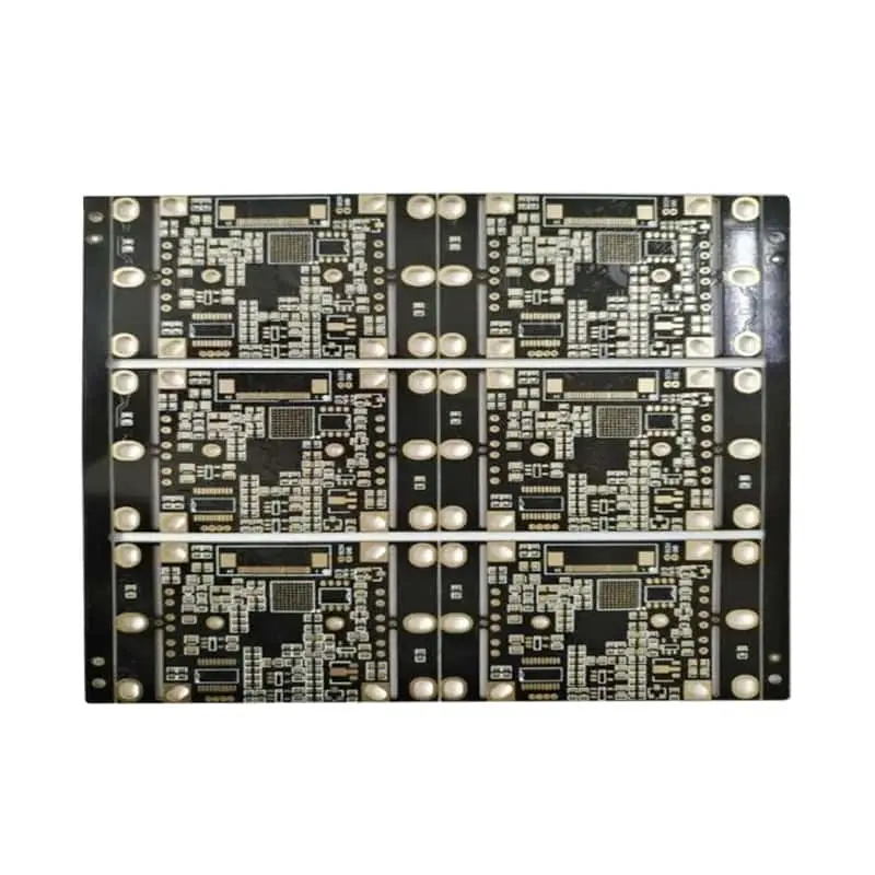
When you’re prototyping high-speed digital, RF, or SerDes-based designs, “close enough” impedance is a recipe for silent failures — reflections, jitter, EMI, and eye-diagram collapse that can burn weeks of debug time. This guide gives you everything a procurement or hardware engineer needs to specify, order, and verify an impedance controlled PCB prototype without guesswork: copy-ready stackup templates, worked calculation examples, ordering checklists, fabrication tolerances, and measurement procedures.
1. Prototype Stackup and Dielectric Selection
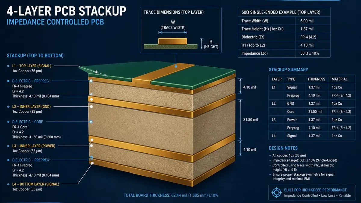
4-Layer Impedance Controlled PCB Prototype Stackup Diagram
A controlled-impedance prototype starts with a stackup your fab house can actually manufacture — and repeat. Below are two common, copy-ready templates.
2-layer (50Ω single-ended, outer microstrip):
| Layer | Material | Thickness |
| L1 Signal | 1 oz copper (35 µm) | 35 µm |
| Prepreg / core dielectric | FR-4, Er ≈ 4.2–4.5 (Tg 150–170) | 1.2 mm (47 mil) |
| L2 Ground / power | 1 oz copper | 35 µm |
Typical result: 50Ω single-ended trace ≈ 110 mil wide — usable for RF feeds and low-speed buses, but rarely for dense digital routing.
4-layer (50Ω single-ended + 100Ω differential):
| Layer | Material | Thickness |
| L1 Signal (microstrip) | 1 oz copper | 35 µm |
| Prepreg 2116 | Er ≈ 4.2–4.4 | 4.2 mil (0.107 mm) |
| L2 Ground | 1 oz copper | 35 µm |
| Core FR-4 | Er ≈ 4.4–4.6 | 39 mil (1.0 mm) |
| L3 Power | 1 oz copper | 35 µm |
| Prepreg 2116 | Er ≈ 4.2–4.4 | 4.2 mil |
| L4 Signal (microstrip) | 1 oz copper | 35 µm |
With L1–L2 spacing of ~4.2 mil, a 50Ω single-ended trace is ≈ 7.5 mil (0.19 mm) wide; a 100Ω differential pair is ≈ 7 mil width / 8 mil gap. These are fab-stable, standard-process values — no premium charges.
Material trade-offs:
Standard FR-4 (Tg 150–170, Er 4.2–4.6) handles prototypes up to ~3–5 Gbps comfortably and is cheapest. Mid-loss FR-4 variants (e.g., Isola 370HR, Panasonic Megtron-class laminates) reduce insertion loss for 5–10+ Gbps links. PTFE/ceramic substrates (Er 2.2–3.5) are reserved for RF above ~10 GHz — expect 3–5× material cost and longer lead times. Per IPC-4101 and IPC-6012 guidance, specify the laminate designation (e.g., FR-4.0 / Tg150) rather than a brand name in your fabrication notes; this keeps you vendor-flexible while locking electrical properties. For quick-turn prototypes, 4.2 mil prepreg and 1 oz copper are the sweet spot: every major shop stocks them and holds Er and thickness tolerances tightly enough for ±10% impedance control.
2. Trace Geometry, Differential Routing, and Via Transitions
Worked example 1 — 50Ω single-ended microstrip.
Use the IPC-2141 approximation: Z₀ ≈ (87 / √(Er + 1.41)) · ln(5.98h / (0.8w + t))
With FR-4 Er = 4.2, dielectric height h = 4.2 mil, copper thickness t = 1.37 mil: Z₀ ≈ (87 / √5.61) · ln(5.98 × 4.2 / (0.8w + 1.37)) ≈ 36.7 · ln(25.1 / (0.8w + 1.37)). Setting Z₀ = 50Ω and solving gives w ≈ 7.5 mil — a standard, fabricable width. For stripline (signal between two ground planes), the same formula with the 2√-stripline variant yields roughly 5.5 mil at h = 8 mil to either plane. Always confirm with your vendor’s 2D field solver; the IPC formula is ±5–10% accurate.
Worked example 2 — 100Ω differential pair.
For edge-coupled microstrip, compute the odd-mode impedance so that 2 × Z_odd ≈ 100Ω. At w = 7 mil, gap = 8 mil, h = 4.2 mil, Er = 4.2, you land at Z_diff ≈ 100Ω. Practical rule of thumb: start with gap ≈ width, then fine-tune via field solver. For 90Ω (USB 3.x, PCIe Gen 3+), widen the pair slightly or reduce gap — most fabs offer 90/100Ω as a standard impedance option at no extra charge.
Routing practices for prototypes:
- Keep the pair coupled for its entire length; gaps between P and N wider than ~2× the dielectric height break coupling and shift impedance locally.
- Match intra-pair length to within 5 mil (0.127 mm) for ≤ 5 Gbps, 2 mil for 10+ Gbps; use serpentine tuning in the uncoupled region only.
- Avoid 90° bends; use 45° or arc bends to keep effective width constant.
- Maintain ≥ 3× line-width clearance from unrelated nets and board edges.
Vias and transitions:
An untamed through-hole via looks like a ~30–60 pH inductance plus ~0.3–0.8 pF capacitance — a significant discontinuity above ~2–3 Gbps. Mitigations: place ground vias within 40 mil of every signal via, use via-in-pad with backdrilling (removes the stub), or specify blind/buried vias for layer-1-to-layer-2 transitions on HDI prototypes. Backdrilling adds one fab step and typically 10–20% cost — specify it in the fab notes whenever via stubs exceed ~1/20th of the signal rise-time length.
3. Fabrication Tolerances, Documentation & Prototype Ordering Checklist
Tolerances turn “impedance control” from a wish into a contract term. Standard industry commitments:
- Impedance tolerance: ±10% is the default for quick-turn; ±5% is achievable on premium services with dedicated coupons. Specifying ±3Ω on a 50Ω line is aggressive — most vendors quote it as ±5%.
- Minimum trace/space: 5/5 mil standard on quick-turn; 4/4 mil on advanced lines (higher cost).
- Drill tolerance: ±2 mil on plated holes; ±1 mil laser (HDI only).
- Dielectric thickness: ±10% on prepreg; this is why coupon-based measurement — not simulation alone — is the contractual verification.
Copy-ready ordering checklist:
[X] Gerbers (RS-274X) + drill files, or ODB++ (preferred for impedance jobs)
[X] Fabrication notes: laminate type/designation, Tg, copper weight per layer
[X] Stackup table with ALL dielectric thicknesses and Er values
[X] For each controlled net class: target impedance, tolerance (e.g., 50Ω ±10%),
layer, trace width, spacing, reference planes
[X] Impedance test coupon request: coupon location (panel edge, specified corner),
coupon design (e.g., 8-inch coupon with each impedance structure,
single-ended and differential sections)
[X] Backdrill / blind via requirements with depth tolerances
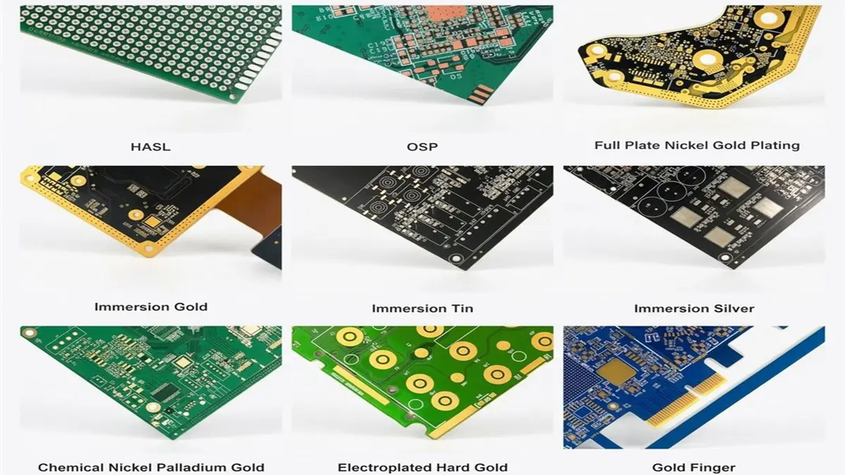
[X] Surface finish (ENIG recommended for high-speed pads)
[X] Panelization / breakaway routing instructions
[X] Quantity, desired lead time, and acceptance criteria
Ask for the coupon TDR data before the boards ship; reputable vendors measure every coupon and include a report.
4. Simulation, Modeling, and Impedance Measurement
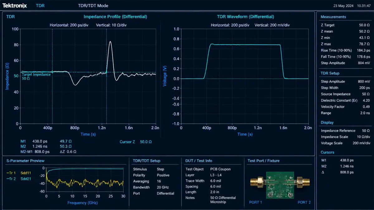
Impedance Controlled PCB Prototype TDR Measurement and Waveform Display
Design-side flow:
Start with a 2D field-solver stackup tool (e.g., Polar Si8000-class calculators, built-in tools in Altium/Cadence) to set width/gap from your fab’s actual dielectric data — not generic Er values. For multi-gigabit links, move to channel simulation (S-parameters, eye diagrams) in HyperLynx, ADS, or open-source alternatives; flag any via transition above 1 dB return loss below your Nyquist frequency and fix it before ordering. Export the final stackup and geometry into your fab notes so the vendor simulates against the same numbers you did.
Measurement-side flow:
Vendors verify impedance two ways:
- TDR (time-domain reflectometry): launches a fast step into the coupon and reads impedance versus distance. This is the contractual standard for prototypes — it directly shows where a discontinuity lives (e.g., a via at 3.2 inches).
- VNA (vector network analyzer): measures S-parameters in frequency domain; required for insertion/return-loss compliance at multi-gigabit rates.
Bandwidth rule: TDR rise time should be ≤ 35 ps for 10+ Gbps coupons, ≤ 100 ps for mainstream prototype verification. Probe/fixture discontinuities must be de-embedded or the launch is measured, not the trace.
A measurement report should include:
Coupon ID and location, target vs. measured impedance per structure (mean, min, max over the coupon length), a TDR plot with cursor markers at discontinuities, instrument and probe details, date, and pass/fail per your tolerance. On a TDR trace, a capacitive dip (via, pad) drops Z momentarily; an inductive bump (narrow neck, void) raises it. A sustained offset means the fab’s Er or thickness differed from your assumptions — negotiate against your acceptance criteria before accepting panels.
5. Cost, Lead Time, and Vendor Specification Templates
What drives cost (in rough order):
- Layer count — 4-layer to 6-layer is typically +40–60%; beyond that, climbing.
- Special laminates — mid-loss +20–40%; PTFE +200–400%.
- Backdrilling / blind vias — +10–30% per extra process.
- Tight impedance tolerance — ±10% included; ±5% adds ~10–15% and requires coupon verification on premium lines.
- Small features — 4/4 mil rules add ~15–25% over 5/5 mil.
Typical quick-turn lead times:
| Service tier | Lead time | Relative cost |
| Super quick-turn | 24–72 hours | ~2–3× standard |
| Fast prototype | 3–5 days | ~1.5× standard |
| Standard prototype | 5–10 business days | baseline |
Copy-ready RFQ / vendor specification template:
TARGET IMPEDANCES:
Net class A (USB/PCIe diff): 90Ω ±10%, L1 & L4, ref L2/L3
Net class B (RF single-end): 50Ω ±10%, L1, ref L2
COUPONS: One per panel, lower-right corner; 200 mm length;
include all controlled structures; TDR report required pre-ship.
STACKUP: Per attached table (4-layer, FR-4 Tg170, 1 oz all layers,
2116 prepreg 4.2 mil)
FEATURES: 5/5 mil min trace/space; 0.3 mm min drill; no backdrill
FINISH: ENIG, 2 µ” Au min
FILES: ODB++ + fabrication drawing; drill file excellon 2
ACCEPTANCE: Impedance per coupon TDR within stated tolerance;
boards conforming IPC-A-600 Class 2
QTY / LEAD TIME: 10 pcs, 5-day standard (quote 24-hr option)
Presenting this template to two or three vendors produces apples-to-apples quotes — and exposes who actually measures coupons versus who just promises impedance.
Ready to Order Your Impedance Controlled Prototype?
Download our free impedance specification template and stackup calculator — the same tables above, formatted for direct inclusion in your fabrication notes. Better still, upload your Gerbers and stackup for a quick-turn quote in under 24 hours: our standard service ships impedance-verified 4-layer prototypes in 24–72 hours, with a TDR test report from every impedance coupon included at no charge. Need to move from prototype to production? Ask about our DFM review and volume-transition program — we’ll lock your stackup and tolerances so production boards match your prototypes exactly.
Request a Quote | Get the Impedance Template Email:pcb@pcbcoming.com
FAQ
What stackup should I use for a 50Ω single-ended prototype on FR-4?
A 4-layer stackup with 4.2 mil (2116) prepreg between L1 signal and L2 ground, 1 oz copper, yields ~7.5 mil traces at 50Ω — a standard, no-premium configuration. For 2-layer boards, use ≥1.2 mm core for ~110 mil 50Ω traces (RF feeds only).
How do I calculate trace width and spacing for 90–100Ω differential impedance?
Use a 2D field solver (Polar, Altium impedance calculator) with your fab’s Er and prepreg thickness. Starting point on 4.2 mil dielectric: 7 mil width / 8 mil gap for 100Ω; slightly wider pair for 90Ω. Verify with the fab before release.
What fabrication tolerances should I specify to ensure controlled impedance?
±10% impedance (default, included), 5/5 mil min trace/space, ±2 mil drill, ±10% dielectric thickness — and always require coupon-based TDR verification. Tighten to ±5% only if your signal integrity budget demands it.
How are impedance measurements performed, and what should the report include?
TDR for impedance-vs-distance (contract standard), VNA for frequency-domain S-parameters. The report must show target vs. measured impedance, TDR plots with discontinuity markers, instrument/probe details, and pass/fail against your tolerance.
What files, coupons, and documentation do vendors need?
Gerber/RS-274X or ODB++, drill files, a fabrication drawing with stackup and Er values, per-net-class impedance specs, and a coupon spec (location, design, TDR requirement). ODB++ reduces stackup miscommunication for impedance jobs.
How do via transitions and backdrilling affect impedance?
Vias add inductance and capacitance that appear as impedance bumps/dips on TDR above ~2–3 Gbps. Mitigate with adjacent ground vias, or specify backdrilling/blind vias when stubs are long relative to the rise time.
How much extra cost and lead time does impedance control add?
Standard ±10% impedance control is typically included in prototype pricing at major vendors. Premium items: ±5% tolerance (+10–15%), backdrilling (+10–30%), and 24–72 hr super quick-turn (~2–3× standard). Standard 5–10 day prototypes with impedance verification add little to nothing over non-controlled boards.
About Author
David Chen https://www.linkedin.com/in/pcbcoming
David Chen is a Senior RF/PCB Process Engineer at Shenzhen Hongda Circuit Technology Co., Ltd., with over 12 years of experience in high-frequency PCB fabrication, impedance-controlled stack-up design, and Rogers/PTFE laminate processing. He also boasts an extensive professional background in PCBA manufacturing, PCBA testing, and PCBA optimization, with specialized expertise in high-precision PCBA fault analysis and rigorous PCBA reliability testing. The author has worked with high-layer-count server PCB fabrication, ultra-low-loss backplane stackups, and thermo-mechanical reliability optimization for AI infrastructure projects involving 112G and 224G PAM4 architectures. Skilled in complex circuit design and cutting-edge advanced PCB manufacturing processes, he delivers solutions that elevate product durability and performance across industrial applications. His technical articles focusing on PCBA manufacturing workflows and testing methodologies are widely cited by industry peers and technical platforms, and have gained attention and recognition from industry colleagues.