Author name: admin

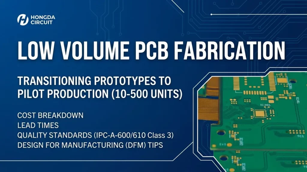
Low Volume Pcb Fabrication Cover Banner

Low-Volume PCB Fabrication & Assembly: Comprehensive Procurement Guide

Low Volume PCB Fabrication requires balancing unit costs, initial setup overhead, turn time, and stringent quality control. Whether you are transitioning an engineering prototype to pilot production (10 to 500 units) or launching a specialized high-mix product, finding the optimal balance between speed and manufacturability is critical to project success. This comprehensive procurement guide provides […]

Low-Volume PCB Fabrication & Assembly: Comprehensive Procurement Guide Read More »
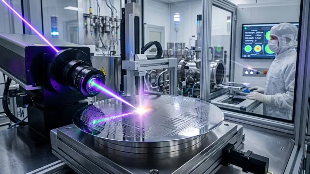
Laser annealing semiconductor process on silicon wafer in cleanroom manufacturing facility

Laser Annealing for Semiconductor Manufacturing: Process Control, Dopant Activation, and Equipment Selection

Laser annealing semiconductor processing delivers localized heating of semiconductor substrates, enabling rapid recrystallization and dopant activation while minimizing thermal damage to adjacent device structures. For semiconductor manufacturers, optimal process tuning relies on multiple critical parameters: laser wavelength, laser fluence, pulse duration, melt depth, material compatibility, target electrical performance, and validated production throughput. Selecting a laser

Laser Annealing for Semiconductor Manufacturing: Process Control, Dopant Activation, and Equipment Selection Read More »

pcb-laser-etching-technology-process

What Is PCB Laser Etching Technology, and How Do You Select the Right Process for Production?

PCB laser etching uses a focused laser beam to selectively modify or remove material during printed circuit board manufacturing. Depending on the process, lasers can remove copper, pattern selected layers, or drill microvias. For OEM buyers, the right solution depends on copper thickness, substrate compatibility, feature size, registration accuracy, production volume, and total manufacturing cost—not

What Is PCB Laser Etching Technology, and How Do You Select the Right Process for Production? Read More »

Double Sided Pcbs Fabrication Guide

Complete Guide to Double-Sided PCBs: Fabrication, Design Rules, and DFM for Procurement

Selecting the optimal printed circuit board (PCB) architecture is a crucial technical and economic decision in electronics manufacturing. While single-sided boards offer lower upfront costs and multilayer boards provide ultra-high density, double-sided PCBs (two-layer PCBs) represent the ideal balance between circuit density, electrical performance, and cost-efficiency. This guide provides engineering teams, procurement specialists, and hardware

Complete Guide to Double-Sided PCBs: Fabrication, Design Rules, and DFM for Procurement Read More »

Reducing Total Cost and Improving ROI with Electronic Manufacturing Solutions

How Do Electronic Manufacturing Solutions Reduce Cost, Improve Quality, and Accelerate Production?

How Do Electronic Manufacturing Solutions Reduce Cost, Improve Quality, and Accelerate Production? Electronic manufacturing solutions reduce production risk by coordinating component sourcing, PCB fabrication, assembly, testing, and delivery under a controlled workflow. Their value depends on measurable outcomes: total cost per accepted unit, first-pass yield, verified test coverage, production readiness, and delivery performance—not simply a

How Do Electronic Manufacturing Solutions Reduce Cost, Improve Quality, and Accelerate Production? Read More »

Learn About Driver Circuit Board Cover

Driver Circuit Board: Design, PCB Manufacturing, Assembly, and Supplier Selection

Driver Circuit Board: Design, PCB Manufacturing, Assembly, and Supplier Selection A driver circuit board converts control signals into the electrical power needed to operate LEDs, motors, power switches, and other electronic loads. For OEMs and industrial equipment manufacturers, selecting the right driver circuit board requires more than matching voltage and current ratings. PCB layout, component

Driver Circuit Board: Design, PCB Manufacturing, Assembly, and Supplier Selection Read More »

Pcb Via Current Calculator Cover

What is a PCB Via Current Calculator and How to Use It in Your Desig

A PCB via current calculator is an engineering tool that estimates how much electrical current a plated through-hole, blind via, or buried via can safely carry before its temperature rise exceeds a specified limit. For procurement teams, design engineers, and hardware program managers sourcing boards in the North American supply chain, this tool answers one

What is a PCB Via Current Calculator and How to Use It in Your Desig Read More »

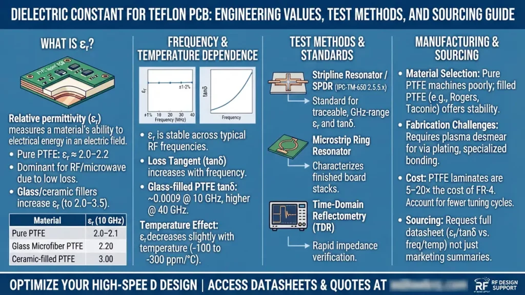
Dielectric Constant for Teflon PCB: Engineering Values, Test Methods, and Sourcing Guide cover image

Dielectric Constant for Teflon PCB: Engineering Values, Test Methods, and Sourcing Guide

Dielectric constant for Teflon PCB is the primary parameter to evaluate when selecting PTFE (Teflon®) laminate for RF, microwave, and high-speed circuit designs — and it is also one of the most frequently misrepresented specifications in the industry. While most competitor product materials broadly claim that PTFE features a low dielectric constant, few provide authentic

Dielectric Constant for Teflon PCB: Engineering Values, Test Methods, and Sourcing Guide Read More »

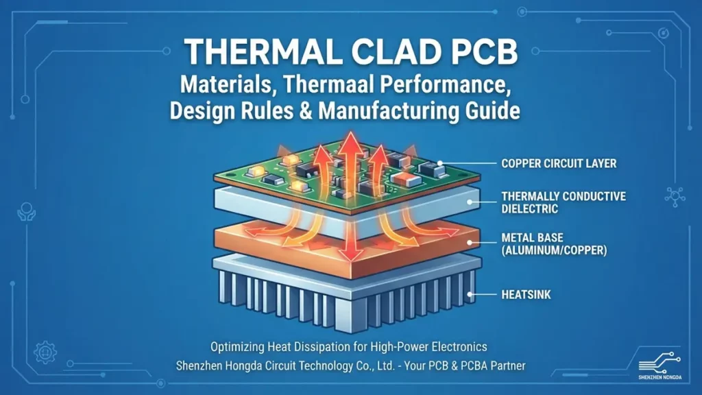
Thermal clad PCB layered stackup showing copper circuit, thermally conductive dielectric, metal base, and heatsink, illustrating heat dissipation in high-power electronics.

Thermal Clad PCB: Materials, Thermal Performance, Design Rules & Manufacturing Guide

A thermal clad PCB is a circuit board designed to transfer heat away from power-generating components through a thermally conductive dielectric and a metal base or heat-spreading structure. It is commonly considered for LED lighting, power conversion, automotive electronics, and high-power communication equipment where conventional FR-4 may not provide sufficient thermal performance. Choosing the right

Thermal Clad PCB: Materials, Thermal Performance, Design Rules & Manufacturing Guide Read More »